 ChipApex | Global Electronic Components Supplier
DG445BDJ
Search Product
Search Post
— IC芯片 | 连接器 | 传感器 | 被动器件 —
Search productSearch post
— IC芯片 | 连接器 | 传感器 | 被动器件 —
Consult the customer manager about the wholesale price.
consultation hotline:86-132-6715-2157
email:[email protected]
Contact the product manager for consultation. One-stop consultation is available.
Do you want a lower wholesale price? Please send us your inquiry and we will reply immediately.
The DG445BDJ is a monolithic quad SPST CMOS analog switch manufactured by Vishay Siliconix in a 16-pin Plastic DIP package. It provides high-speed switching with a typical turn-on time of 120 ns and a maximum of 300 ns, alongside a typical on-resistance of 45 Ω (maximum 80 Ω). The device operates from dual supplies up to ±15 V or a single supply up to 12 V, drawing a maximum supply current of 1 µA. It features low charge injection of 1 pC and TTL/CMOS-compatible logic inputs.
Verify the specific ordering suffix against the manufacturer's official documentation to confirm package type and compliance status. Confirm availability as distribution channels may vary. Ensure the component meets the required environmental specifications for the intended application environment before finalizing procurement.
Select this component when low distortion and high speed are required for analog signal routing. Verify that the 45 Ω typical on-resistance meets the system's voltage drop requirements. Ensure the logic input levels align with the control circuitry, as the device supports both TTL and CMOS standards.
The DG445BDJ belongs to the DG444B/DG445B series, which are improved upgrades to the original DG444/DG445 models. These devices utilize a high-voltage silicon-gate process with an epitaxial layer to prevent latchup. The DG445B variant specifically offers inverted logic control compared to the DG444B.
DG444BDJ serves as a logical alternative if non-inverted logic control is preferred over the DG445B's inverted configuration. Both share identical electrical characteristics and pinouts within the same package family.
The primary difference is the logic control. The DG444B turns ON when the input is Logic High (≥ 2.4 V), while the DG445B turns ON when the input is Logic Low (≤ 0.8 V).
With dual supplies of ±15 V, the analog signal range is -15 V to +15 V. With a single supply of 12 V, the range is 0 V to 12 V.
Signals on the Source (S) or Drain (D) pins exceeding V+ or V- will be clamped by internal diodes. The forward diode current must be limited to the maximum current ratings to prevent damage.
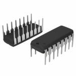 DG445BDJ
The activity of extra discounts on wholesale prices is in full swing…
Please fill in your contact information and we will send you the latest wholesale price list.





