 ChipApex | Global Electronic Components Supplier
DG9409DN-T1-E4
Search Product
Search Post
— IC芯片 | 连接器 | 传感器 | 被动器件 —
Search productSearch post
— IC芯片 | 连接器 | 传感器 | 被动器件 —
Consult the customer manager about the wholesale price.
consultation hotline:86-132-6715-2157
email:[email protected]
Contact the product manager for consultation. One-stop consultation is available.
Do you want a lower wholesale price? Please send us your inquiry and we will reply immediately.
The DG9409DN-T1-E4 is a dual 4-channel differential analog multiplexer manufactured by Vishay Siliconix using BiCMOS technology. It connects one of four differential inputs to a common dual output via a 2-bit binary address (A0, A1). The device operates on single supplies from 2.7 V to 12 V or dual supplies from ±3 V to ±6 V. Key electrical parameters include a maximum on-resistance of 25.5 Ω at 3 V supply, transition times up to 182 ns, and off-isolation of -80 dB. It features break-before-make switching, TTL/CMOS compatibility, and is housed in a 16-pin QFN package.
Verify the specific ordering suffix against current Vishay documentation to confirm lead-free terminations and package variations. Confirm availability status as distribution channels may list this component as obsolete or restricted. Ensure the selected variant matches the required operating temperature range and voltage specifications for the target application environment.
Select the DG9409DN-T1-E4 when differential signal routing is required within a compact surface-mount footprint. Evaluate the on-resistance flatness and leakage currents against the specific supply voltage conditions of the design. Ensure the digital control interface aligns with the system's logic voltage levels, particularly at lower supply voltages where thresholds shift.
This component belongs to the DG940x series of precision low-voltage analog multiplexers. It shares the same die and core architecture as the DG9408 but differs in channel count and configuration. Both devices utilize the same 16-pin QFN package and are designed for applications requiring high accuracy and low power consumption in portable electronics.
DG9408DN-T1-E4: Single-ended 8-channel version with identical pinout and electrical characteristics.
The EN pin enables or disables all switches simultaneously. When EN is low, all switches are turned off regardless of the address inputs.
Signals on the source (S) or drain (D) pins exceeding the supply rails (V+ or V-) will be clamped by internal diodes to protect the device.
The typical charge injection is 29 pC at room temperature with a 1 nF load capacitance, though it varies with supply voltage and temperature.
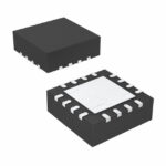 DG9409DN-T1-E4
The activity of extra discounts on wholesale prices is in full swing…
Please fill in your contact information and we will send you the latest wholesale price list.





