 ChipApex | Global Electronic Components Supplier

SEARCH
Search Product
Search Post
— IC芯片 | 连接器 | 传感器 | 被动器件 —
Search productSearch post
— IC芯片 | 连接器 | 传感器 | 被动器件 —
Consult the customer manager about the wholesale price.
consultation hotline:86-132-6715-2157
email:[email protected]
Contact the product manager for consultation. One-stop consultation is available.
Do you want a lower wholesale price? Please send us your inquiry and we will reply immediately.
DS90LV110TMTCX/NOPB is listed in the Clock Buffers, Drivers range at ChipApex. The manufacturer field lists Texas Instruments. Its product description is IC CLK BUF 1:10 400MHZ 28TSSOP. Review the specifications below when checking this part for your BOM.
The DS90LV110TMTCX/NOPB is a Texas Instruments LVDS interface integrated circuit designed as a 1-to-10 data and clock distributor. It features one receiver and ten drivers, supporting data rates up to 400 Mb/s. The device operates on a single 3.3 V power supply with a voltage range of 3.0 V to 3.6 V. It accepts LVDS inputs and provides LVDS outputs. Key electrical parameters include a propagation delay of 3.9 ns and a maximum input voltage differential of ±100 mV. The component is housed in a 28-pin TSSOP package and functions within an operating temperature range of -40°C to +85°C.
Verify the specific suffix 'TMTCX' against the manufacturer's official datasheet to confirm the tape-and-reel packaging configuration and temperature grade. Ensure compatibility with existing PCB footprints for the 28-pin TSSOP package. Confirm that the 3.3 V operating voltage aligns with the target system's power domain requirements before integration.
Select this component when a single LVDS source needs to drive ten distinct loads simultaneously. The 400 Mb/s speed rating suits applications requiring moderate bandwidth with low skew. Consider the 28-pin TSSOP package constraints for board space. Verify that the load capacitance at each of the ten output nodes remains within the driver's specifications to maintain signal integrity at the maximum data rate.
This part belongs to the DS90LV110AT series of LVDS line drivers and receivers from Texas Instruments. It serves as a buffer and distributor within the broader family of Low Voltage Differential Signaling interface solutions. The device complements other components like the DS90LV011 or DS90LV048 by providing multi-output distribution capabilities rather than simple point-to-point conversion or quad buffering.
Direct pin-to-pin replacements within the same series may include variants with different suffixes indicating packaging changes, such as tube versus reel options. Cross-model substitution requires verifying that the alternative device supports the required 1-to-10 fan-out ratio and 400 Mb/s data rate. Ensure the replacement maintains LVDS input/output compatibility.
Explore related parts through Clock/Timing, Integrated Circuits (ICs), all product categories, ChipApex homepage.
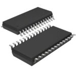 DS90LV110TMTCX/NOPB
DS90LV110TMTCX/NOPB is listed in the Clock Buffers, Drivers range at ChipApex. The manufacturer field lists Texas Instruments. Its product description is IC CLK BUF…
Read More
DS90LV110TMTCX/NOPB is listed in the Clock Buffers, Drivers range at ChipApex. The manufacturer field lists Texas Instruments. Its product description is IC CLK BUF…
Read More
DS90LV110TMTCX/NOPB is listed in the Clock Buffers, Drivers range at ChipApex. The manufacturer field lists Texas Instruments. Its product description is IC CLK BUF…
Read More
Understand how a comparator switches at a voltage threshold, why hysteresis prevents chatter, and which output and input specs matter.
Read More
DS90LV110TMTCX/NOPB is listed in the Clock Buffers, Drivers range at ChipApex. The manufacturer field lists Texas Instruments. Its product description is IC CLK BUF…
Read More
DS90LV110TMTCX/NOPB is listed in the Clock Buffers, Drivers range at ChipApex. The manufacturer field lists Texas Instruments. Its product description is IC CLK BUF…
Read More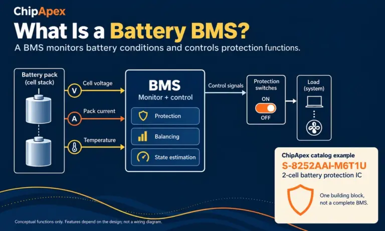
Learn what a battery BMS does, how protection differs from charging, and which pack specifications to check when sourcing BMS components through ChipApex.
Read More
DS90LV110TMTCX/NOPB is listed in the Clock Buffers, Drivers range at ChipApex. The manufacturer field lists Texas Instruments. Its product description is IC CLK BUF…
Read More
DS90LV110TMTCX/NOPB is listed in the Clock Buffers, Drivers range at ChipApex. The manufacturer field lists Texas Instruments. Its product description is IC CLK BUF…
Read More
DS90LV110TMTCX/NOPB is listed in the Clock Buffers, Drivers range at ChipApex. The manufacturer field lists Texas Instruments. Its product description is IC CLK BUF…
Read More
DS90LV110TMTCX/NOPB is listed in the Clock Buffers, Drivers range at ChipApex. The manufacturer field lists Texas Instruments. Its product description is IC CLK BUF…
Read More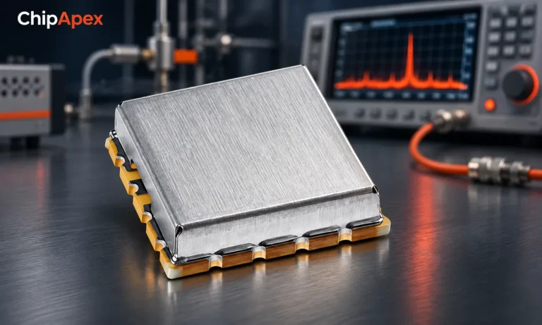
Understand voltage controlled oscillator tuning, phase noise and PLL operation. Check supply noise, output loading and requirements before selection.
Read More
The activity of extra discounts on wholesale prices is in full swing…
Please fill in your contact information and we will send you the latest wholesale price list.





