ChipApex | Global Electronic Components Supplier
FST33X257QSP
Search Product
Search Post
— IC芯片 | 连接器 | 传感器 | 被动器件 —
Search productSearch post
— IC芯片 | 连接器 | 传感器 | 被动器件 —
Consult the customer manager about the wholesale price.
consultation hotline:86-132-6715-2157
email:[email protected]
Contact the product manager for consultation. One-stop consultation is available.
Do you want a lower wholesale price? Please send us your inquiry and we will reply immediately.
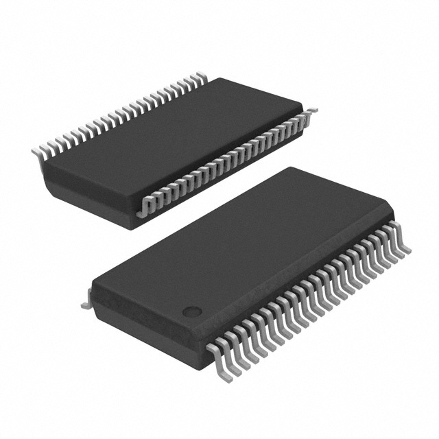
The FST33X257QSP is a 24:12 high-speed CMOS TTL-compatible multiplexer/demultiplexer bus switch. It features a low on-resistance of 4Ω typical, allowing inputs to connect to outputs without adding propagation delay or generating ground bounce noise. The device operates with a supply voltage range of 4.0V to 5.5V and supports an operating temperature from -40°C to +85°C. It utilizes a 48-lead Quarter Size Very Small Outline Package (QVSOP).
Verify the specific ordering code suffix to confirm package type and reel configuration. Ensure the component meets the required thermal and electrical specifications for the intended operating environment. Confirm compatibility with existing design constraints before finalizing procurement decisions.
Select this component when a 24-to-12 channel multiplexing solution is required with low on-resistance characteristics. Consider the QVSOP package size for space-constrained designs. Verify that the TTL-compatible control inputs align with the system's logic voltage levels.
This part belongs to the Fairchild Switch family, which embodies proven switch technology used in previous bus switch products. It is designed to provide efficient signal routing with minimal impact on signal integrity, suitable for various digital interface applications.
Check for direct pin-to-pin replacements within the same product family. Verify that any substitute component matches the 24:12 configuration and package dimensions. Ensure electrical parameters such as on-resistance and propagation delay meet or exceed the original specifications.
When OE_x is LOW, the select pin connects the A Port to the selected B Port output. When HIGH, the switch is OPEN, creating a high-impedance state between the two ports.
The input leakage current is specified as ±1.0 µA maximum at VCC = 5.5V and VIN ranging from 0V to 5.5V.
 FST33X257QSP
The activity of extra discounts on wholesale prices is in full swing…
Please fill in your contact information and we will send you the latest wholesale price list.