 ChipApex | Global Electronic Components Supplier

SEARCH
Search Product
Search Post
— IC芯片 | 连接器 | 传感器 | 被动器件 —
Search productSearch post
— IC芯片 | 连接器 | 传感器 | 被动器件 —
Consult the customer manager about the wholesale price.
consultation hotline:86-132-6715-2157
email:[email protected]
Contact the product manager for consultation. One-stop consultation is available.
Do you want a lower wholesale price? Please send us your inquiry and we will reply immediately.
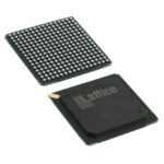
LFE2M35E-5F256I is listed in the Field Programmable Gate Array range at ChipApex. The manufacturer field lists Lattice Semiconductor Corporation. Its product description is IC FPGA 140 I/O 256FBGA. Review the specifications below when checking this part for your BOM.
The LFE2M35E-5F256I is a Field Programmable Gate Array (FPGA) from the Lattice ECP2M family, manufactured by Lattice Semiconductor Corporation. It features 34,000 logic elements and 4,250 LABs/CLBs with 2,151,424 total RAM bits. The device supports up to 140 I/Os and operates within a supply voltage range of 1.14V to 1.26V. Packaged in a 256-FPBGA (17x17 mm) surface-mount format, it is rated for industrial temperature ranges of 0°C to 85°C TJ.
Verify the specific suffix 'I' indicates the industrial temperature grade variant when sourcing. Confirm package dimensions match the 256-FPBGA specification. Check RoHS compliance status against current manufacturing revisions. Ensure design tools support the ECP2M family architecture prior to procurement.
Select this model for applications requiring embedded SERDES capabilities within the ECP2M series. Compare logic density requirements against other family members like the LFE250E. Verify power consumption constraints align with the 1.2V core voltage operation. Ensure thermal management suits the specified junction temperature range.
This component belongs to the Lattice ECP2M FPGA family, which integrates embedded SERDES technology. The family targets high-performance connectivity and signal processing applications. It combines significant logic resources with dedicated DSP blocks and memory structures for system-level integration.
Consider the LFE2M35SE-5F256C for commercial temperature variants. Evaluate the LFE2M35E-5FN484C for higher I/O counts in larger packages. Verify pin compatibility before substituting different package options within the same logic density tier.
Explore related parts through Embedded, Integrated Circuits (ICs), all product categories, ChipApex homepage.
 LFE2M35E-5F256I
LFE2M35E-5F256I is listed in the Field Programmable Gate Array range at ChipApex. The manufacturer field lists Lattice Semiconductor Corporation. Its product description is IC…
Read More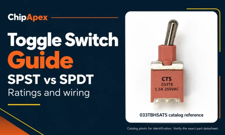
Compare SPST and SPDT toggle switches, understand AC/DC ratings, and follow wiring examples. Check contact action, mounting and parts in the ChipApex catalog.
Read More
LFE2M35E-5F256I is listed in the Field Programmable Gate Array range at ChipApex. The manufacturer field lists Lattice Semiconductor Corporation. Its product description is IC…
Read More
LFE2M35E-5F256I is listed in the Field Programmable Gate Array range at ChipApex. The manufacturer field lists Lattice Semiconductor Corporation. Its product description is IC…
Read More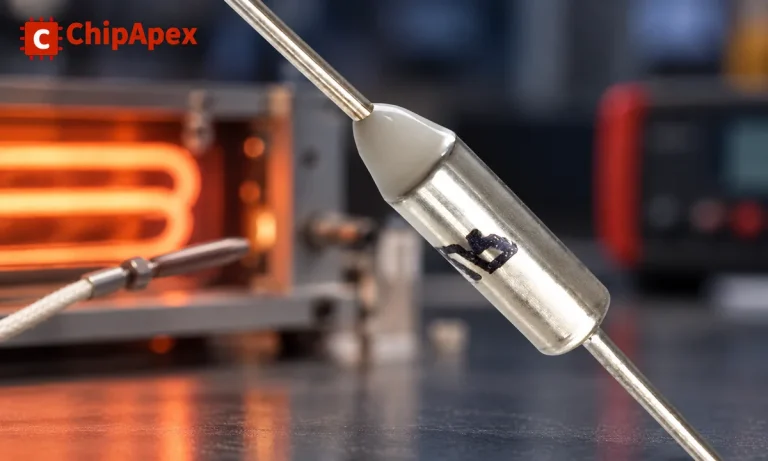
Understand thermal fuse operation, Tf, Th and Tm, electrical ratings and mounting. Check temperature limits and replacement requirements for your design.
Read More
LFE2M35E-5F256I is listed in the Field Programmable Gate Array range at ChipApex. The manufacturer field lists Lattice Semiconductor Corporation. Its product description is IC…
Read More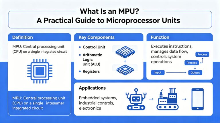
LFE2M35E-5F256I is listed in the Field Programmable Gate Array range at ChipApex. The manufacturer field lists Lattice Semiconductor Corporation. Its product description is IC…
Read More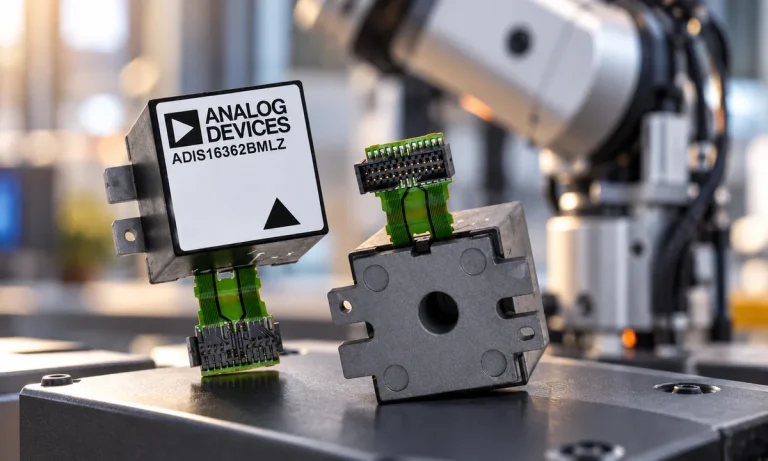
Learn what an IMU measures, how accelerometers and gyroscopes work together, why orientation estimates drift, and what to compare.
Read More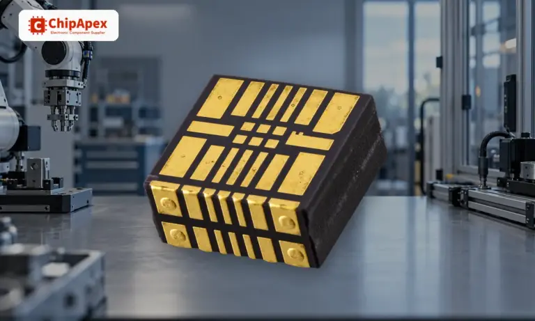
See how a MEMS gyroscope measures angular rate, why its angle estimate drifts, and which range, noise, interface and temperature specs to compare.
Read More
LFE2M35E-5F256I is listed in the Field Programmable Gate Array range at ChipApex. The manufacturer field lists Lattice Semiconductor Corporation. Its product description is IC…
Read More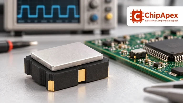
Compare RC, crystal and MEMS oscillator circuits. Check ppm, jitter, load capacitance, startup margin and output compatibility before choosing a clock source.
Read More
LFE2M35E-5F256I is listed in the Field Programmable Gate Array range at ChipApex. The manufacturer field lists Lattice Semiconductor Corporation. Its product description is IC…
Read More
The activity of extra discounts on wholesale prices is in full swing…
Please fill in your contact information and we will send you the latest wholesale price list.






