ChipApex | Global Electronic Components Supplier

SEARCH
Search Product
Search Post
— IC芯片 | 连接器 | 传感器 | 被动器件 —
Search productSearch post
— IC芯片 | 连接器 | 传感器 | 被动器件 —
Consult the customer manager about the wholesale price.
consultation hotline:86-132-6715-2157
email:[email protected]
Contact the product manager for consultation. One-stop consultation is available.
Do you want a lower wholesale price? Please send us your inquiry and we will reply immediately.
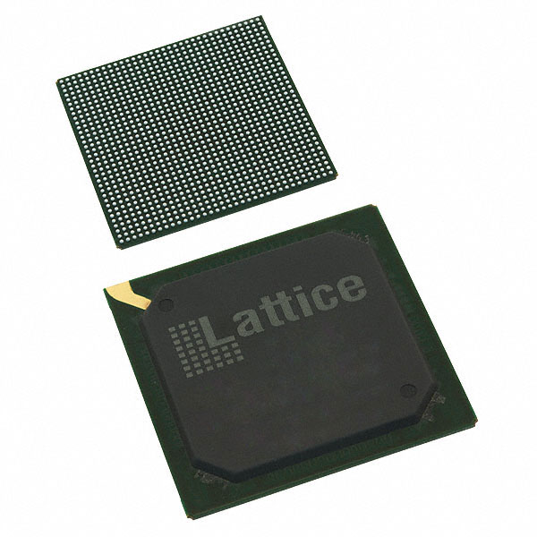
LFE3-95EA-7FN1156I is listed in the Field Programmable Gate Array range at ChipApex. The manufacturer field lists Lattice Semiconductor Corporation. Its product description is IC FPGA 490 I/O 1156FBGA. Review the specifications below when checking this part for your BOM.
The LFE3-95EA-7FN1156I is a Field Programmable Gate Array (FPGA) from the Lattice ECP3 family, manufactured by Lattice Semiconductor Corporation. It features 92,000 logic elements and 46,000 Adaptive Logic Modules (ALMs). The device includes 4.32 Mbits of embedded memory, comprising 188 kbits of distributed RAM and 4,420 kbits of Embedded Block RAM (EBR). It supports up to 490 I/Os with SERDES capabilities operating at data rates up to 3.2 Gb/s. The component operates within a supply voltage range of 1.14 V to 1.26 V and functions in industrial temperature conditions from -40°C to +100°C. It is housed in an FPBGA-1156 package.
Verify the specific suffix '7' corresponds to the required speed grade and that the 'I' designation matches the intended industrial temperature range requirements. Confirm the FPBGA-1156 package dimensions align with the target PCB footprint constraints. Ensure compatibility with the design toolchain version supporting the ECP3 family architecture before finalizing procurement orders.
Select this model when the design requires approximately 92K LUTs and significant embedded memory capacity within a single FPGA die. Consider the 1156-pin package availability if board space permits larger footprints compared to smaller variants like the FN484 or FN672. Evaluate power consumption profiles against the system's thermal management capabilities, noting the 1.2V core voltage requirement.
This component belongs to the Lattice ECP3 series, which targets cost-sensitive applications needing moderate density and low power consumption. It serves as a bridge between lower-density ICE40 devices and higher-end CrossLink or MachXO families. The ECP3 architecture emphasizes efficiency, making it suitable for edge computing tasks where power and area are critical constraints.
Direct pin-to-pin replacements within the same package are limited due to varying logic densities. The LFE3-95EA-8FN1156I offers a different speed grade but maintains identical pinout and functionality. Designers should verify timing closure requirements when substituting speed grades, as electrical characteristics may differ slightly despite functional equivalence.
Explore related parts through Embedded, Integrated Circuits (ICs), all product categories, ChipApex homepage.
 LFE3-95EA-7FN1156I
LFE3-95EA-7FN1156I is listed in the Field Programmable Gate Array range at ChipApex. The manufacturer field lists Lattice Semiconductor Corporation. Its product description is IC…
Read More
LFE3-95EA-7FN1156I is listed in the Field Programmable Gate Array range at ChipApex. The manufacturer field lists Lattice Semiconductor Corporation. Its product description is IC…
Read More
See how a MEMS gyroscope measures angular rate, why its angle estimate drifts, and which range, noise, interface and temperature specs to compare.
Read More
LFE3-95EA-7FN1156I is listed in the Field Programmable Gate Array range at ChipApex. The manufacturer field lists Lattice Semiconductor Corporation. Its product description is IC…
Read More
LFE3-95EA-7FN1156I is listed in the Field Programmable Gate Array range at ChipApex. The manufacturer field lists Lattice Semiconductor Corporation. Its product description is IC…
Read More
LFE3-95EA-7FN1156I is listed in the Field Programmable Gate Array range at ChipApex. The manufacturer field lists Lattice Semiconductor Corporation. Its product description is IC…
Read More
LFE3-95EA-7FN1156I is listed in the Field Programmable Gate Array range at ChipApex. The manufacturer field lists Lattice Semiconductor Corporation. Its product description is IC…
Read More
LFE3-95EA-7FN1156I is listed in the Field Programmable Gate Array range at ChipApex. The manufacturer field lists Lattice Semiconductor Corporation. Its product description is IC…
Read More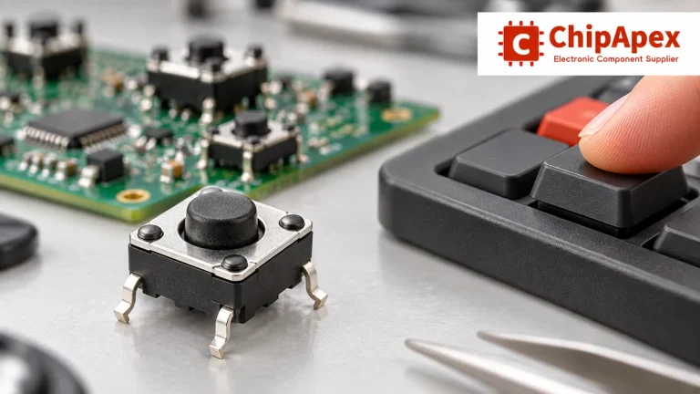
Understand tactile switches, PCB and keyboard differences, four-pin wiring, debounce, force, travel and replacement checks for reliable control inputs.
Read More
LFE3-95EA-7FN1156I is listed in the Field Programmable Gate Array range at ChipApex. The manufacturer field lists Lattice Semiconductor Corporation. Its product description is IC…
Read More
LFE3-95EA-7FN1156I is listed in the Field Programmable Gate Array range at ChipApex. The manufacturer field lists Lattice Semiconductor Corporation. Its product description is IC…
Read More
LFE3-95EA-7FN1156I is listed in the Field Programmable Gate Array range at ChipApex. The manufacturer field lists Lattice Semiconductor Corporation. Its product description is IC…
Read More
The activity of extra discounts on wholesale prices is in full swing…
Please fill in your contact information and we will send you the latest wholesale price list.