 ChipApex | Global Electronic Components Supplier

SEARCH
Search Product
Search Post
— IC芯片 | 连接器 | 传感器 | 被动器件 —
Search productSearch post
— IC芯片 | 连接器 | 传感器 | 被动器件 —
Consult the customer manager about the wholesale price.
consultation hotline:86-132-6715-2157
email:[email protected]
Contact the product manager for consultation. One-stop consultation is available.
Do you want a lower wholesale price? Please send us your inquiry and we will reply immediately.
LFX125EC-03F256C is listed in the Field Programmable Gate Array range at ChipApex. The manufacturer field lists Lattice Semiconductor Corporation. Its product description is FPGA, 484 CLBS, 139000 GATES. Review the specifications below when checking this part for your BOM.
The LFX125EC-03F256C is a Field Programmable Gate Array (FPGA) belonging to the Lattice CrossLink-NX family. It features 484 Configurable Logic Blocks (CLBs) and approximately 139,000 logic gates. The device operates with a maximum clock frequency of 420 MHz and exhibits a CLB-maximum combinational delay of 0.56 ns. It is housed in a 516-pin Plastic Flat Ball Grid Array (FPBGA) package measuring 23 x 23 mm with a 1 mm pitch. The component supports an operating temperature range of -40°C to +100°C.
Verify the specific suffix '03' corresponds to the required speed grade and '-F256' matches the 516-pin FPBGA package dimensions. Confirm RoHS compliance status and lead-free pin availability through official manufacturer documentation prior to ordering.
Compare against other CrossLink-NX variants based on I/O count requirements and SERDES channel availability. Ensure the selected device meets the thermal dissipation needs of the target application given the dense packaging.
This component is part of the Lattice CrossLink-NX series, designed for bridging legacy interfaces with modern high-speed protocols. It targets applications requiring moderate logic density with significant serial connectivity capabilities.
Direct substitutes within the same family include LFX125EC-03FN516C or LFX125EC-03FT256C if package variations are acceptable. Verify pinout compatibility before implementation.
Explore related parts through Embedded, Integrated Circuits (ICs), all product categories, ChipApex homepage.
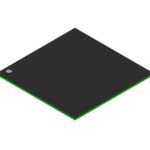 LFX125EC-03F256C
Choose an ADC converter by resolution, sample rate, noise and input design. Review practical tradeoffs and prepare component requirements for ChipApex.
Read More
LFX125EC-03F256C is listed in the Field Programmable Gate Array range at ChipApex. The manufacturer field lists Lattice Semiconductor Corporation. Its product description is FPGA,…
Read More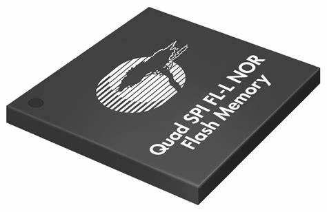
LFX125EC-03F256C is listed in the Field Programmable Gate Array range at ChipApex. The manufacturer field lists Lattice Semiconductor Corporation. Its product description is FPGA,…
Read More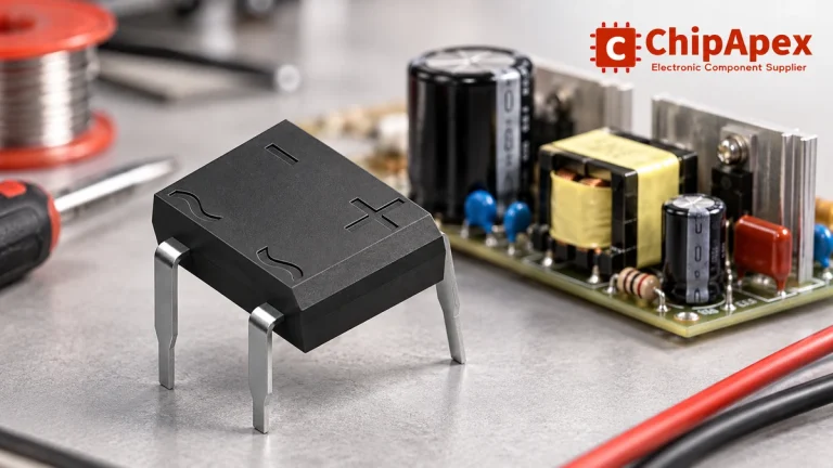
Select a bridge rectifier by reverse voltage, capacitor charging current, startup surge and cooling. Work through a stated DC voltage and ripple example.
Read More
Choose a vibration sensor for machine monitoring. Compare sensing methods, bandwidth, noise and mounting, then define the signal-chain requirements.
Read More
LFX125EC-03F256C is listed in the Field Programmable Gate Array range at ChipApex. The manufacturer field lists Lattice Semiconductor Corporation. Its product description is FPGA,…
Read More
LFX125EC-03F256C is listed in the Field Programmable Gate Array range at ChipApex. The manufacturer field lists Lattice Semiconductor Corporation. Its product description is FPGA,…
Read More
LFX125EC-03F256C is listed in the Field Programmable Gate Array range at ChipApex. The manufacturer field lists Lattice Semiconductor Corporation. Its product description is FPGA,…
Read More
LFX125EC-03F256C is listed in the Field Programmable Gate Array range at ChipApex. The manufacturer field lists Lattice Semiconductor Corporation. Its product description is FPGA,…
Read More
Choose logic inverter ICs by thresholds, supply, output drive and delay. Compare standard and Schmitt-trigger inputs, power sequencing and replacement checks.
Read More
Compare Pt100 and Pt1000 RTDs, two-, three- and four-wire connections, excitation and self-heating. Build an error budget from element to reported temperature.
Read More
LFX125EC-03F256C is listed in the Field Programmable Gate Array range at ChipApex. The manufacturer field lists Lattice Semiconductor Corporation. Its product description is FPGA,…
Read More
The activity of extra discounts on wholesale prices is in full swing…
Please fill in your contact information and we will send you the latest wholesale price list.






