ChipApex | Global Electronic Components Supplier

SEARCH
Search Product
Search Post
— IC芯片 | 连接器 | 传感器 | 被动器件 —
Search productSearch post
— IC芯片 | 连接器 | 传感器 | 被动器件 —
Consult the customer manager about the wholesale price.
consultation hotline:86-132-6715-2157
email:[email protected]
Contact the product manager for consultation. One-stop consultation is available.
Do you want a lower wholesale price? Please send us your inquiry and we will reply immediately.
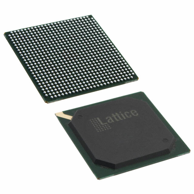
LFXP2-30E-5F672C is listed in the Field Programmable Gate Array range at ChipApex. The manufacturer field lists Lattice Semiconductor Corporation. Its product description is IC FPGA 472 I/O 672FPBGA. Review the specifications below when checking this part for your BOM.
The LFXP2-30E-5F672C is a Field Programmable Gate Array from the Lattice LFXP2 series, manufactured by Lattice Semiconductor Corporation. It features 30,000 logic elements and 15,000 Adaptive Logic Modules within a 672-ball FineLine BGA package. The device includes 885 kbit of embedded block RAM and supports a maximum operating frequency of 420 MHz. It operates at a core voltage of 1.2 V with a range of 1.14 V to 1.26 V. The component is rated for commercial temperature operation between 0°C and +85°C.
Verify the specific speed grade suffix '5' against the official Lattice datasheet to confirm timing characteristics. Ensure the FPBGA-672 package dimensions match the target PCB footprint requirements. Confirm RoHS compliance status through the manufacturer's current documentation before finalizing procurement specifications.
Select this model when a balance of moderate logic density and high I/O count is required in a single package. Compare total memory capacity against application buffer needs. Evaluate the 672-pin form factor against available board real estate constraints relative to alternative pin counts.
This component belongs to the LFXP2 family, which targets mid-range FPGA applications requiring efficient power consumption and reliable performance. The series is designed for industrial and telecom sectors where robustness and connectivity are prioritized over extreme high-end processing speeds.
Consult Lattice official cross-reference tools for verified compatible devices. Verify pinout compatibility and electrical specifications before substituting with other LFXP2 variants or different families.
Explore related parts through Embedded, Integrated Circuits (ICs), all product categories, ChipApex homepage.
 LFXP2-30E-5F672C

LFXP2-30E-5F672C is listed in the Field Programmable Gate Array range at ChipApex. The manufacturer field lists Lattice Semiconductor Corporation. Its product description is IC…
Read More
LFXP2-30E-5F672C is listed in the Field Programmable Gate Array range at ChipApex. The manufacturer field lists Lattice Semiconductor Corporation. Its product description is IC…
Read More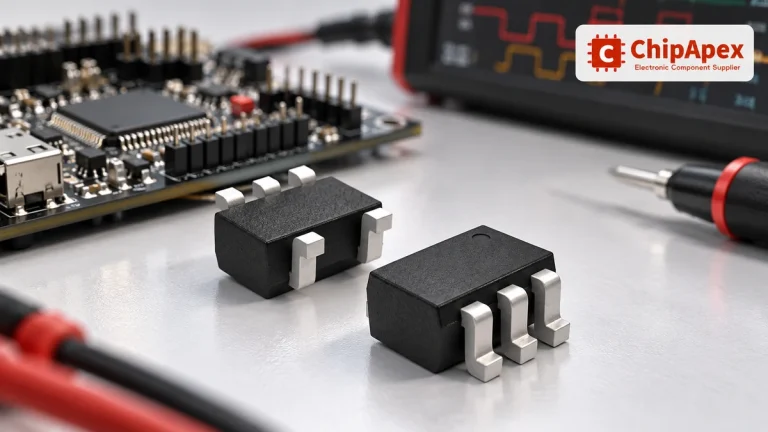
Choose logic inverter ICs by thresholds, supply, output drive and delay. Compare standard and Schmitt-trigger inputs, power sequencing and replacement checks.
Read More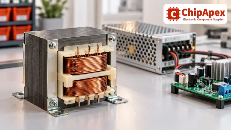
Select power transformers by input frequency, secondary VA, rectifier load, isolation, regulation and inrush. Build a clearer specification for your next RFQ.
Read More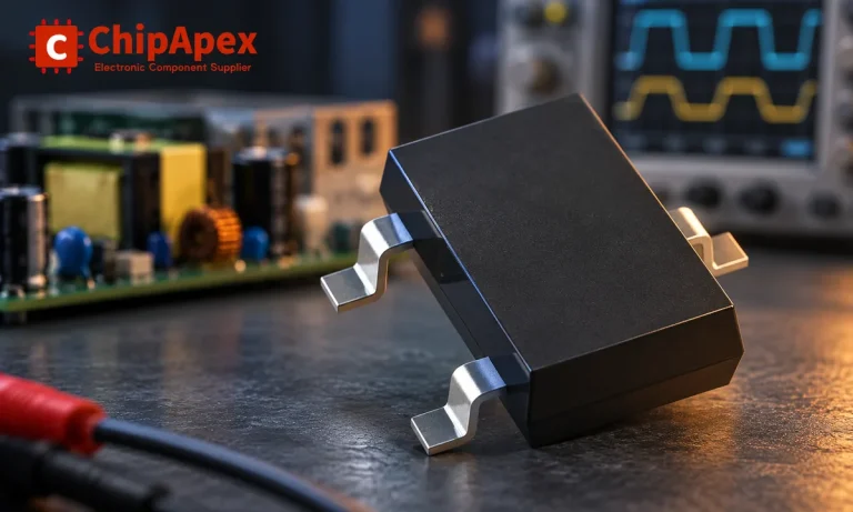
Learn how rectifiers convert AC to DC, compare half-wave and bridge circuits, and select voltage, current, recovery and thermal ratings for your design.
Read More
LFXP2-30E-5F672C is listed in the Field Programmable Gate Array range at ChipApex. The manufacturer field lists Lattice Semiconductor Corporation. Its product description is IC…
Read More
LFXP2-30E-5F672C is listed in the Field Programmable Gate Array range at ChipApex. The manufacturer field lists Lattice Semiconductor Corporation. Its product description is IC…
Read More
Select MOV varistors by continuous voltage, clamping behavior, surge waveform and repetition. Check thermal disconnection, fuse coordination and replacements.
Read More
LFXP2-30E-5F672C is listed in the Field Programmable Gate Array range at ChipApex. The manufacturer field lists Lattice Semiconductor Corporation. Its product description is IC…
Read More
LFXP2-30E-5F672C is listed in the Field Programmable Gate Array range at ChipApex. The manufacturer field lists Lattice Semiconductor Corporation. Its product description is IC…
Read More
LFXP2-30E-5F672C is listed in the Field Programmable Gate Array range at ChipApex. The manufacturer field lists Lattice Semiconductor Corporation. Its product description is IC…
Read More
LFXP2-30E-5F672C is listed in the Field Programmable Gate Array range at ChipApex. The manufacturer field lists Lattice Semiconductor Corporation. Its product description is IC…
Read More
The activity of extra discounts on wholesale prices is in full swing…
Please fill in your contact information and we will send you the latest wholesale price list.