 ChipApex | Global Electronic Components Supplier

SEARCH
Search Product
Search Post
— IC芯片 | 连接器 | 传感器 | 被动器件 —
Search productSearch post
— IC芯片 | 连接器 | 传感器 | 被动器件 —
Consult the customer manager about the wholesale price.
consultation hotline:86-132-6715-2157
email:[email protected]
Contact the product manager for consultation. One-stop consultation is available.
Do you want a lower wholesale price? Please send us your inquiry and we will reply immediately.
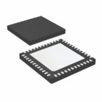
LMK00301SQE/NOPB is listed in the Clock Buffers, Drivers range at ChipApex. The manufacturer field lists Texas Instruments. Its product description is IC CLK BUFFER 3:11 3.1GHZ 48WQFN. Review the specifications below when checking this part for your BOM.
The LMK00301SQE/NOPB is a high-performance clock buffer and level translator manufactured by Texas Instruments. It features a single circuit with a 3:11 input-to-output ratio, supporting maximum frequencies of 3.1 GHz for both input and output signals. The device accepts multiple input logic standards including CML, HCSL, HSTL, LVDS, LVPECL, SSTL, and crystal inputs. Outputs are configurable to HCSL, LVCMOS, LVDS, or LVPECL levels. It operates on a supply voltage range of 3.15 V to 3.45 V with a typical operating current of 13.5 mA. The component is housed in a 48-WQFN package with exposed pad and functions within an industrial temperature range of -40°C to +85°C.
Verify the specific suffix code against the manufacturer's latest documentation to confirm pinout and electrical characteristics. The 'SQE' designation indicates a specific tape and reel packaging configuration. Confirm moisture sensitivity level (MSL 3) handling requirements prior to assembly. Ensure the ordering part number matches the exact package variant required for the PCB footprint.
Select this component when a single input source must drive up to eleven outputs with varying logic levels. Verify that the system power supply remains within the 3.15 V to 3.45 V range to ensure optimal performance. Consider the 48-WQFN thermal pad requirements for adequate heat dissipation. Compare input/output voltage swing requirements against the supported HCSL, LVDS, and LVPECL options to determine necessary termination resistors.
This device belongs to the LMK00301 family of low-jitter clock buffers. It serves as a versatile interface solution for converting and distributing high-frequency clock signals across mixed-voltage domains. The NOPB suffix indicates lead-free construction compliant with RoHS directives. It is distinct from other LMK series parts by its specific 3:11 ratio and broad input/output flexibility.
Direct replacements within the same family include LMK00301SQX/NOPB, which shares identical electrical specifications but may differ in packaging quantity or reel type. Verify pin-to-pin compatibility before substitution. Other LMK series devices offer different input/output ratios and should be evaluated based on specific channel count requirements.
Explore related parts through Clock/Timing, Integrated Circuits (ICs), all product categories, ChipApex homepage.
 LMK00301SQE/NOPB

LMK00301SQE/NOPB is listed in the Clock Buffers, Drivers range at ChipApex. The manufacturer field lists Texas Instruments. Its product description is IC CLK BUFFER…
Read More
LMK00301SQE/NOPB is listed in the Clock Buffers, Drivers range at ChipApex. The manufacturer field lists Texas Instruments. Its product description is IC CLK BUFFER…
Read More
LMK00301SQE/NOPB is listed in the Clock Buffers, Drivers range at ChipApex. The manufacturer field lists Texas Instruments. Its product description is IC CLK BUFFER…
Read More
LMK00301SQE/NOPB is listed in the Clock Buffers, Drivers range at ChipApex. The manufacturer field lists Texas Instruments. Its product description is IC CLK BUFFER…
Read More
LMK00301SQE/NOPB is listed in the Clock Buffers, Drivers range at ChipApex. The manufacturer field lists Texas Instruments. Its product description is IC CLK BUFFER…
Read More
Choose an AC to DC converter by input range, output demand, isolation, efficiency and thermal derating. Compare architectures and check installation needs.
Read More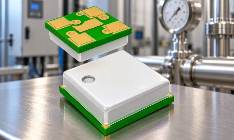
Learn how a pressure transducer converts pressure into voltage, current, or digital output, and compare pressure references and key selection specs.
Read More
LMK00301SQE/NOPB is listed in the Clock Buffers, Drivers range at ChipApex. The manufacturer field lists Texas Instruments. Its product description is IC CLK BUFFER…
Read More
LMK00301SQE/NOPB is listed in the Clock Buffers, Drivers range at ChipApex. The manufacturer field lists Texas Instruments. Its product description is IC CLK BUFFER…
Read More
LMK00301SQE/NOPB is listed in the Clock Buffers, Drivers range at ChipApex. The manufacturer field lists Texas Instruments. Its product description is IC CLK BUFFER…
Read More
LMK00301SQE/NOPB is listed in the Clock Buffers, Drivers range at ChipApex. The manufacturer field lists Texas Instruments. Its product description is IC CLK BUFFER…
Read More
LMK00301SQE/NOPB is listed in the Clock Buffers, Drivers range at ChipApex. The manufacturer field lists Texas Instruments. Its product description is IC CLK BUFFER…
Read More
The activity of extra discounts on wholesale prices is in full swing…
Please fill in your contact information and we will send you the latest wholesale price list.





