ChipApex | Global Electronic Components Supplier

SEARCH
Search Product
Search Post
— IC芯片 | 连接器 | 传感器 | 被动器件 —
Search productSearch post
— IC芯片 | 连接器 | 传感器 | 被动器件 —
Consult the customer manager about the wholesale price.
consultation hotline:86-132-6715-2157
email:[email protected]
Contact the product manager for consultation. One-stop consultation is available.
Do you want a lower wholesale price? Please send us your inquiry and we will reply immediately.
LTC2053HDD#PBF is listed in the Instrumentation, Op Amps, Buffer Amps range at ChipApex. The manufacturer field lists Analog Devices Inc.. Its product description is IC OPAMP ZERO-DRIFT 1 CIRC 8DFN. Review the specifications below when checking this part for your BOM.
The LTC2053HDD#PBF is a precision, rail-to-rail, zero-drift instrumentation amplifier in an 8-lead (3mm × 3mm) plastic DFN package. It features a typical CMRR of 116dB independent of gain and a maximum input offset voltage of 10µV with drift under 50nV/°C. Gain is programmable via two external resistors. The device operates on single supplies from 2.7V to 5.5V or dual ±5.5V supplies, consuming approximately 750µA to 1.3mA depending on supply voltage.
Verify the specific H-grade temperature rating (-40°C to 125°C) against application requirements. Confirm the DD package dimensions match the PCB footprint. Ensure power supply bypassing capacitors are placed close to the V+ and V– pins to maintain stability due to the internal sampling circuitry.
Select this component when high DC accuracy and low drift are critical. The H-grade variant supports extended industrial temperatures up to 125°C. Use the standard LTC2053 if synchronization to an external clock is not required, as the SYNC version offers that feature but requires careful handling of the CLK pin if unused.
This part belongs to the LTC2053 family of zero-drift instrumentation amplifiers. It shares architectural similarities with the LTC2053-SYNC but lacks the external clock synchronization capability. The H-grade designation indicates an extended operating temperature range compared to C and I grades.
LTC2053HDD#TRPBF
The gain is set by two external resistors connected between the RG pin and the inverting input, following the formula G = 1 + R2/R1.
Input charging currents occur during each sampling period. If source resistance is less than 10kΩ, no significant DC errors result from these currents.
Explore related parts through Amplifiers, Linear, Integrated Circuits (ICs), all product categories.
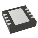 LTC2053HDD#PBF
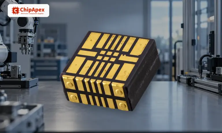
See how a MEMS gyroscope measures angular rate, why its angle estimate drifts, and which range, noise, interface and temperature specs to compare.
Read More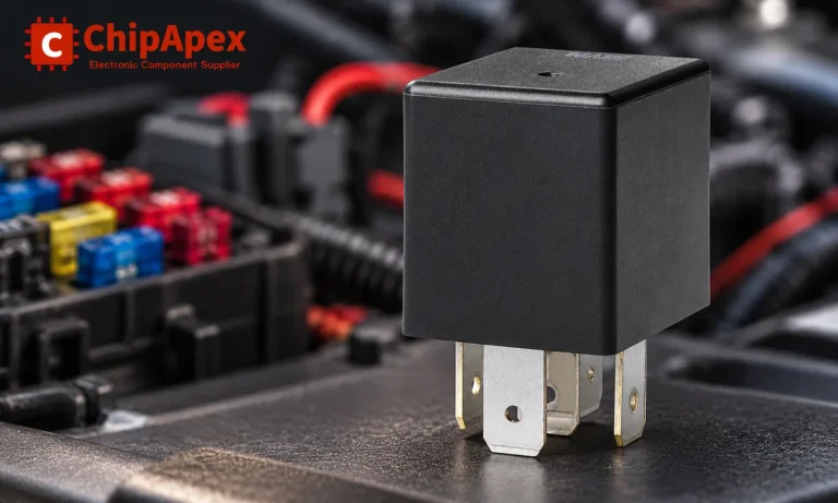
Learn the relay definition, coil and contact operation, NO and NC forms, load ratings and suppression choices. Compare mechanical, reed and solid-state types.
Read More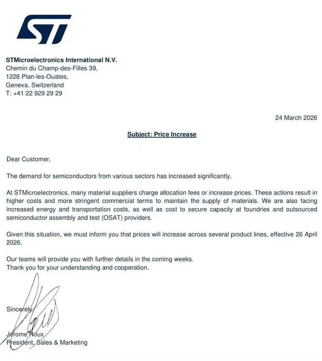
LTC2053HDD#PBF is listed in the Instrumentation, Op Amps, Buffer Amps range at ChipApex. The manufacturer field lists Analog Devices Inc.. Its product description is…
Read More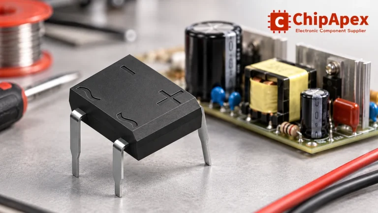
Select a bridge rectifier by reverse voltage, capacitor charging current, startup surge and cooling. Work through a stated DC voltage and ripple example.
Read More
LTC2053HDD#PBF is listed in the Instrumentation, Op Amps, Buffer Amps range at ChipApex. The manufacturer field lists Analog Devices Inc.. Its product description is…
Read More
LTC2053HDD#PBF is listed in the Instrumentation, Op Amps, Buffer Amps range at ChipApex. The manufacturer field lists Analog Devices Inc.. Its product description is…
Read More
LTC2053HDD#PBF is listed in the Instrumentation, Op Amps, Buffer Amps range at ChipApex. The manufacturer field lists Analog Devices Inc.. Its product description is…
Read More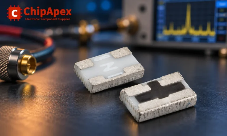
Understand RF attenuator dB values, fixed and programmable types, impedance, power limits and noise tradeoffs before choosing parts for an RF signal path.
Read More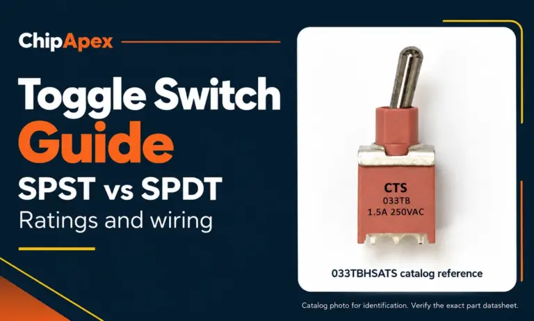
Compare SPST and SPDT toggle switches, understand AC/DC ratings, and follow wiring examples. Check contact action, mounting and parts in the ChipApex catalog.
Read More
LTC2053HDD#PBF is listed in the Instrumentation, Op Amps, Buffer Amps range at ChipApex. The manufacturer field lists Analog Devices Inc.. Its product description is…
Read More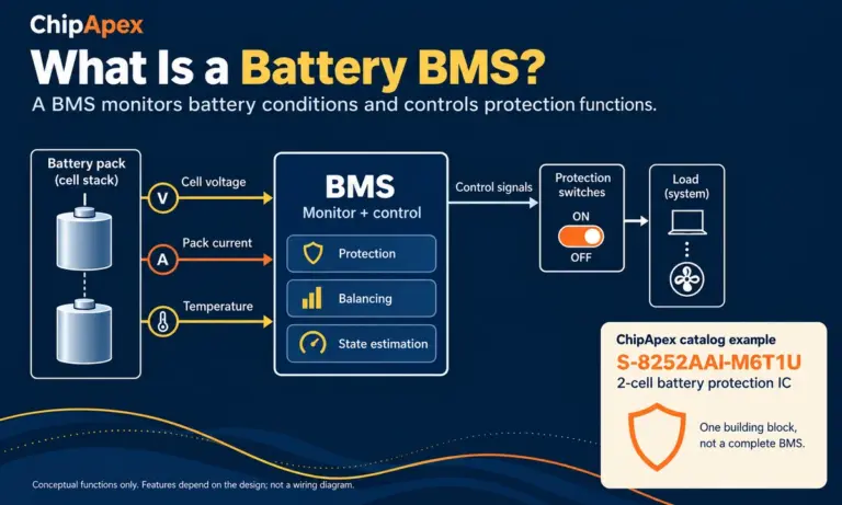
Learn what a battery BMS does, how protection differs from charging, and which pack specifications to check when sourcing BMS components through ChipApex.
Read More
LTC2053HDD#PBF is listed in the Instrumentation, Op Amps, Buffer Amps range at ChipApex. The manufacturer field lists Analog Devices Inc.. Its product description is…
Read More
The activity of extra discounts on wholesale prices is in full swing…
Please fill in your contact information and we will send you the latest wholesale price list.