 ChipApex | Global Electronic Components Supplier
LTC2642IDD-14#PBF
Search Product
Search Post
— IC芯片 | 连接器 | 传感器 | 被动器件 —
Search productSearch post
— IC芯片 | 连接器 | 传感器 | 被动器件 —
Consult the customer manager about the wholesale price.
consultation hotline:86-132-6715-2157
email:[email protected]
Contact the product manager for consultation. One-stop consultation is available.
Do you want a lower wholesale price? Please send us your inquiry and we will reply immediately.
The LTC2642IDD-14#PBF is a 14-bit unbuffered voltage output digital-to-analog converter (DAC) from Analog Devices. It operates on a single 2.7V to 5.5V supply with a typical current consumption of 120µA. The device features a 3-wire SPI/Microwire compatible serial interface supporting clock rates up to 50MHz. Key electrical specifications include a settling time of 1µs, ±0.5 LSB DNL, and ±0.5 LSB INL over the industrial temperature range of -40°C to +85°C. The DAC output swings from 0V to VREF, and the part includes matched scaling resistors for bipolar operation with an external op amp.
Verify the package type is the 10-lead 3mm x 3mm DFN (DD) as specified by the IDD suffix. Confirm the temperature grade corresponds to the Industrial range (-40°C to +85°C). Ensure the #PBF suffix indicates lead-free finish compliance. Check that the specific revision matches the required performance characteristics for your application.
Select this model when bipolar output capability is required alongside 14-bit precision. Unlike the LTC2641, the LTC2642 includes internal RFB and INV pins for connecting to an external amplifier to generate a -VREF to +VREF swing. Ensure the load resistance is greater than 60kΩ to maintain linearity in unbuffered mode, or use an external buffer if lower impedance driving is needed.
This component belongs to the LTC2641/LTC2642 family of high-resolution DACs. The LTC2642 variant is distinguished by its 10-pin configuration and integrated bipolar scaling resistors, whereas the LTC2641 offers 8 pins for unipolar applications only. Both share similar architecture and interface protocols but differ in pinout and power-on reset behavior.
Public confirmed substitute part numbers are not available in the provided documentation.
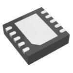 LTC2642IDD-14#PBF
The activity of extra discounts on wholesale prices is in full swing…
Please fill in your contact information and we will send you the latest wholesale price list.







