 ChipApex | Global Electronic Components Supplier

SEARCH
Search Product
Search Post
— IC芯片 | 连接器 | 传感器 | 被动器件 —
Search productSearch post
— IC芯片 | 连接器 | 传感器 | 被动器件 —
Consult the customer manager about the wholesale price.
consultation hotline:86-132-6715-2157
email:[email protected]
Contact the product manager for consultation. One-stop consultation is available.
Do you want a lower wholesale price? Please send us your inquiry and we will reply immediately.
PI6C10810HE is listed in the Clock Buffers, Drivers range at ChipApex. The manufacturer field lists Diodes Incorporated. Its product description is IC CLK BUFFER 1:10 250MHZ 20SSOP. Review the specifications below when checking this part for your BOM.
The PI6C10810HE is a high-speed, low-noise, non-inverting split 1-to-10 clock buffer manufactured by Diodes Incorporated. It supports supply voltages of 1.2V, 1.5V, 1.8V, and 2.5V with a maximum operating frequency of 250 MHz at 2.5V. The device features three independent power banks: Bank A (CLK0-4) on VDDA, Bank B (CLK7-9) on VDDB, and Bank C (CLK5-6) on VDDC. It provides low output skew, propagation delay under 2.0 ns at 2.5V, and additive jitter of 50 ps. The component is housed in a 20-pin SSOP package.
Verify the specific ordering suffix 'H' corresponds to the 20-pin, 209-mil wide SSOP package as defined in the datasheet. Confirm that the 'E' suffix indicates lead-free and green compliant materials. Ensure compatibility with the required supply voltage range of 1.2V to 2.5V for the target application design.
Select this component when a single input must drive ten outputs with minimal skew across different voltage banks. Consider the 250 MHz limit at 2.5V or reduced frequencies at lower voltages (e.g., 150 MHz at 1.2V). Verify that the 20-pin SSOP footprint fits the PCB layout constraints compared to TSSOP or QSOP alternatives.
The PI6C10810HE belongs to the PI6C10810 family of networking clock buffers. The 'HE' suffix specifically denotes the Pb-free, Green 20-pin SSOP package variant. Other variants include LE (TSSOP) and QE (QSOP), sharing identical electrical characteristics but differing in physical package dimensions.
Direct replacements within the same family include PI6C10810LE (20-TSSOP) and PI6C10810QE (20-QSOP). These share the same pinout and electrical specifications but require different footprints. Cross-vendor substitutes are not verified in the provided documentation.
Explore related parts through Clock/Timing, Integrated Circuits (ICs), all product categories, ChipApex homepage.
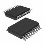 PI6C10810HE
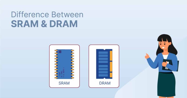
PI6C10810HE is listed in the Clock Buffers, Drivers range at ChipApex. The manufacturer field lists Diodes Incorporated. Its product description is IC CLK BUFFER…
Read More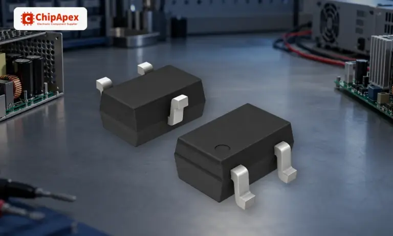
Learn how a diode conducts, how to identify anode and cathode, and when to choose rectifier, TVS, Zener or photodiode types for a circuit.
Read More
PI6C10810HE is listed in the Clock Buffers, Drivers range at ChipApex. The manufacturer field lists Diodes Incorporated. Its product description is IC CLK BUFFER…
Read More
PI6C10810HE is listed in the Clock Buffers, Drivers range at ChipApex. The manufacturer field lists Diodes Incorporated. Its product description is IC CLK BUFFER…
Read More
PI6C10810HE is listed in the Clock Buffers, Drivers range at ChipApex. The manufacturer field lists Diodes Incorporated. Its product description is IC CLK BUFFER…
Read More
PI6C10810HE is listed in the Clock Buffers, Drivers range at ChipApex. The manufacturer field lists Diodes Incorporated. Its product description is IC CLK BUFFER…
Read More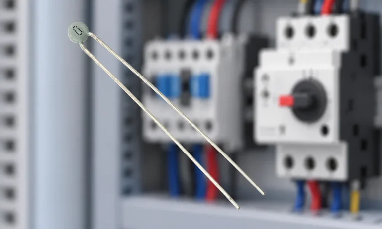
Learn why PTC resistance rises with temperature, how it differs from NTC, and which ratings matter for sensing and protection.
Read More
PI6C10810HE is listed in the Clock Buffers, Drivers range at ChipApex. The manufacturer field lists Diodes Incorporated. Its product description is IC CLK BUFFER…
Read More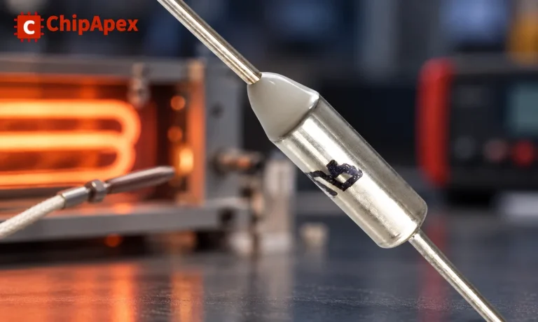
Understand thermal fuse operation, Tf, Th and Tm, electrical ratings and mounting. Check temperature limits and replacement requirements for your design.
Read More
PI6C10810HE is listed in the Clock Buffers, Drivers range at ChipApex. The manufacturer field lists Diodes Incorporated. Its product description is IC CLK BUFFER…
Read More
PI6C10810HE is listed in the Clock Buffers, Drivers range at ChipApex. The manufacturer field lists Diodes Incorporated. Its product description is IC CLK BUFFER…
Read More
Find out when a bare shock switch needs a pull resistor, when an MCU internal pull-up is enough, and why sensor modules and piezo…
Read More
The activity of extra discounts on wholesale prices is in full swing…
Please fill in your contact information and we will send you the latest wholesale price list.





