 ChipApex | Global Electronic Components Supplier

SEARCH
Search Product
Search Post
— IC芯片 | 连接器 | 传感器 | 被动器件 —
Search productSearch post
— IC芯片 | 连接器 | 传感器 | 被动器件 —
Consult the customer manager about the wholesale price.
consultation hotline:86-132-6715-2157
email:[email protected]
Contact the product manager for consultation. One-stop consultation is available.
Do you want a lower wholesale price? Please send us your inquiry and we will reply immediately.
SCAN18245TSSCX is listed in the Buffers, Drivers, Receivers, Transceivers range at ChipApex. The manufacturer field lists onsemi. Its product description is IC TXRX NON-INVERT 5.5V 56SSOP. Review the specifications below when checking this part for your BOM.
The SCAN18245TSSCX is a non-inverting transceiver with 3-STATE outputs, compliant with IEEE 1149.1 (JTAG). It features dual 9-bit bytes with separate data inputs and byte-oriented output enable and direction control signals. Operating at 4.5V to 5.5V, it provides TTL-compatible inputs and reduced-swing outputs capable of driving 50 Ω transmission lines. The device includes boundary-scan test logic and a Test Access Port for system verification.
Verify the obsolete status of this component before procurement planning. Confirm availability of parameter-equivalent substitutes such as the SN74ABT16863DL series from Texas Instruments. Ensure design updates accommodate potential lead time variations associated with alternative sourcing or lifecycle transitions.
Select this device for systems requiring JTAG-compliant boundary scan integration alongside high-speed bidirectional buffering. Evaluate the 56-lead SSOP package constraints against board space limitations. Consider the specific drive capabilities for 50 Ω transmission lines when designing interface circuits for reliable signal integrity.
This component belongs to the SCAN product family, characterized by integrated test access ports. It serves as a bridge between standard logic interfaces and boundary-scan architectures. The device facilitates both functional data transfer and diagnostic testing within complex electronic systems.
Public confirmed substitute part numbers include SN74ABT16863DL and SN74ABT16863DLR from Texas Instruments. These are listed as parameter-equivalent alternatives in distributor databases.
Direction pins DIR1 and DIR2 control data flow; LOW enables B to A, while HIGH enables A to B.
G1 and G2 are output enable pins that place ports in a high impedance condition when set to HIGH.
Explore related parts through Logic, Integrated Circuits (ICs), all product categories, ChipApex homepage.
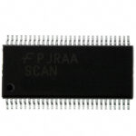 SCAN18245TSSCX

Compare RC, crystal and MEMS oscillator circuits. Check ppm, jitter, load capacitance, startup margin and output compatibility before choosing a clock source.
Read More
SCAN18245TSSCX is listed in the Buffers, Drivers, Receivers, Transceivers range at ChipApex. The manufacturer field lists onsemi. Its product description is IC TXRX NON-INVERT…
Read More
SCAN18245TSSCX is listed in the Buffers, Drivers, Receivers, Transceivers range at ChipApex. The manufacturer field lists onsemi. Its product description is IC TXRX NON-INVERT…
Read More
Choose a DIP switch by contact type, coded positions, footprint and signal ratings. Check logic polarity, assembly conditions and PCB configuration behavior.
Read More
SCAN18245TSSCX is listed in the Buffers, Drivers, Receivers, Transceivers range at ChipApex. The manufacturer field lists onsemi. Its product description is IC TXRX NON-INVERT…
Read More
SCAN18245TSSCX is listed in the Buffers, Drivers, Receivers, Transceivers range at ChipApex. The manufacturer field lists onsemi. Its product description is IC TXRX NON-INVERT…
Read More
SCAN18245TSSCX is listed in the Buffers, Drivers, Receivers, Transceivers range at ChipApex. The manufacturer field lists onsemi. Its product description is IC TXRX NON-INVERT…
Read More
SCAN18245TSSCX is listed in the Buffers, Drivers, Receivers, Transceivers range at ChipApex. The manufacturer field lists onsemi. Its product description is IC TXRX NON-INVERT…
Read More
Learn what an IMU measures, how accelerometers and gyroscopes work together, why orientation estimates drift, and what to compare.
Read More
SCAN18245TSSCX is listed in the Buffers, Drivers, Receivers, Transceivers range at ChipApex. The manufacturer field lists onsemi. Its product description is IC TXRX NON-INVERT…
Read More
SCAN18245TSSCX is listed in the Buffers, Drivers, Receivers, Transceivers range at ChipApex. The manufacturer field lists onsemi. Its product description is IC TXRX NON-INVERT…
Read More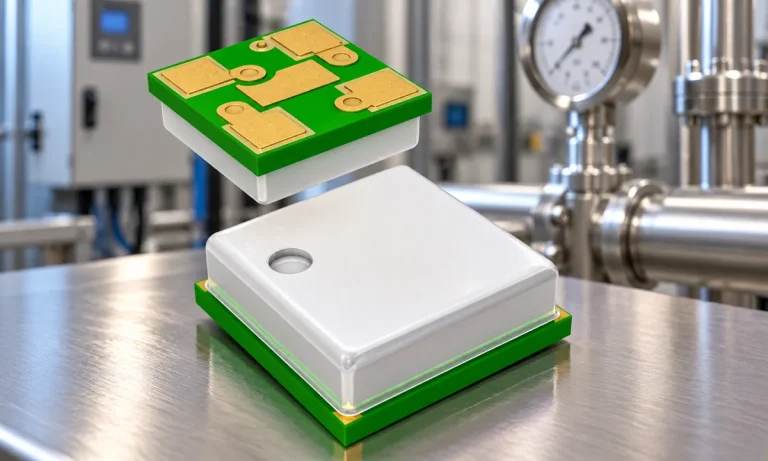
Learn how a pressure transducer converts pressure into voltage, current, or digital output, and compare pressure references and key selection specs.
Read More
The activity of extra discounts on wholesale prices is in full swing…
Please fill in your contact information and we will send you the latest wholesale price list.





