 ChipApex | Global Electronic Components Supplier

SEARCH
Search Product
Search Post
— IC芯片 | 连接器 | 传感器 | 被动器件 —
Search productSearch post
— IC芯片 | 连接器 | 传感器 | 被动器件 —
Consult the customer manager about the wholesale price.
consultation hotline:86-132-6715-2157
email:[email protected]
Contact the product manager for consultation. One-stop consultation is available.
Do you want a lower wholesale price? Please send us your inquiry and we will reply immediately.
SIT92184AA-Y is listed in the Clock Buffers, Drivers range at ChipApex. The manufacturer field lists SiTime. Its product description is -40C TO 125C, 8PIN, 2020, 1.8V-3. Review the specifications below when checking this part for your BOM.
The SiT92184AA-Y is an Automotive Grade 1, AEC-Q100 qualified high-performance LVCMOS clock buffer. It provides a 1:4 output configuration with a maximum operating frequency of 200 MHz and supports supply voltages from 1.8 V to 3.3 V. The device features very low additive phase jitter of less than 50 fs RMS and pin-to-pin skew under 50 ps. Packaged in an 8-pin, 2 x 2 mm DFN, it includes integrated serial termination for 50 Ω channels and synchronous glitch-free output enable functionality.
Verify the package type matches the required land pattern. Confirm that the 8-DFN 2x2mm footprint aligns with the PCB design guidelines provided in the datasheet. Ensure the power supply sequencing meets the requirements for VDD levels above 1.8V.
Select this component when automotive reliability (AEC-Q100 Grade 1) and low jitter are critical. The 3.3 V tolerant CLKIN input allows direct interfacing with higher voltage logic without level shifting. Verify current consumption against the specific operating frequency and load capacitance tables.
The SiT92184 family consists of high-performance LVCMOS clock buffers designed for demanding timing applications. The AA suffix indicates the Automotive Grade 1 variant, which operates reliably across the -40°C to +125°C temperature range. This series replaces discrete buffering solutions with a single, compact IC.
This is a specialized automotive-grade buffer. Direct replacements must match the 1:4 LVCMOS topology, 200 MHz speed, and 8-DFN package. Verify if alternative suppliers offer AEC-Q100 qualification and comparable jitter specifications.
The SiT92184 supports a maximum frequency (FMAX) of 200 MHz.
Yes, it features a synchronous glitch-free output enable (OE) function to eliminate incorrect output clock cycles during enable/disable transitions.
The CLKIN input is 3.3 V tolerant, allowing it to accept clock signals up to 3.3 V even if the core supply (VDD) is lower.
Explore related parts through Clock/Timing, Integrated Circuits (ICs), all product categories, ChipApex homepage.
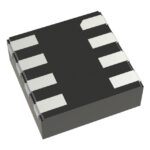 SIT92184AA-Y
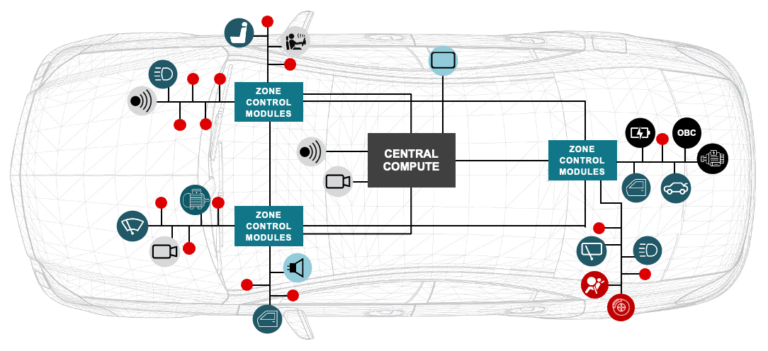
SIT92184AA-Y is listed in the Clock Buffers, Drivers range at ChipApex. The manufacturer field lists SiTime. Its product description is -40C TO 125C, 8PIN,…
Read More
SIT92184AA-Y is listed in the Clock Buffers, Drivers range at ChipApex. The manufacturer field lists SiTime. Its product description is -40C TO 125C, 8PIN,…
Read More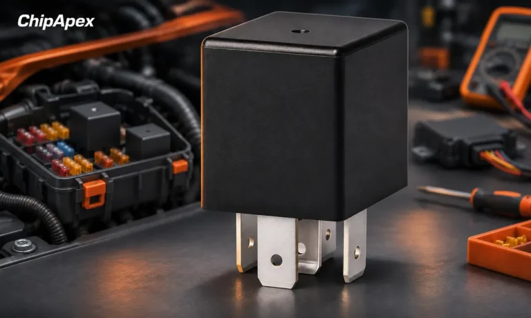
Understand automotive relay terminals, coil suppression and load ratings. Check inrush, socket compatibility and temperature before selecting a replacement.
Read More
SIT92184AA-Y is listed in the Clock Buffers, Drivers range at ChipApex. The manufacturer field lists SiTime. Its product description is -40C TO 125C, 8PIN,…
Read More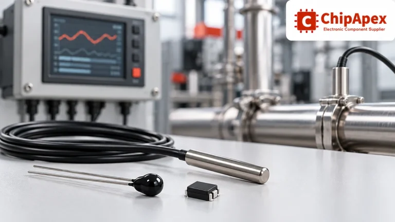
Compare thermistors, RTDs, thermocouples and temperature ICs. Learn how range, accuracy, response, interfaces and mounting affect component selection.
Read More
SIT92184AA-Y is listed in the Clock Buffers, Drivers range at ChipApex. The manufacturer field lists SiTime. Its product description is -40C TO 125C, 8PIN,…
Read More
SIT92184AA-Y is listed in the Clock Buffers, Drivers range at ChipApex. The manufacturer field lists SiTime. Its product description is -40C TO 125C, 8PIN,…
Read More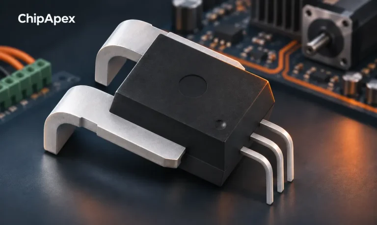
Compare Hall, shunt, current transformer and Rogowski sensing. Check AC/DC capability, accuracy, isolation, heat and response before selecting a sensor.
Read More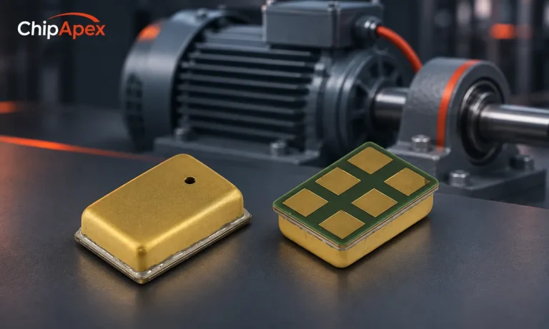
Choose a vibration sensor for machine monitoring. Compare sensing methods, bandwidth, noise and mounting, then define the signal-chain requirements.
Read More
SIT92184AA-Y is listed in the Clock Buffers, Drivers range at ChipApex. The manufacturer field lists SiTime. Its product description is -40C TO 125C, 8PIN,…
Read More
SIT92184AA-Y is listed in the Clock Buffers, Drivers range at ChipApex. The manufacturer field lists SiTime. Its product description is -40C TO 125C, 8PIN,…
Read More
SIT92184AA-Y is listed in the Clock Buffers, Drivers range at ChipApex. The manufacturer field lists SiTime. Its product description is -40C TO 125C, 8PIN,…
Read More
The activity of extra discounts on wholesale prices is in full swing…
Please fill in your contact information and we will send you the latest wholesale price list.





