 ChipApex | Global Electronic Components Supplier

SEARCH
Search Product
Search Post
— IC芯片 | 连接器 | 传感器 | 被动器件 —
Search productSearch post
— IC芯片 | 连接器 | 传感器 | 被动器件 —
Consult the customer manager about the wholesale price.
consultation hotline:86-132-6715-2157
email:[email protected]
Contact the product manager for consultation. One-stop consultation is available.
Do you want a lower wholesale price? Please send us your inquiry and we will reply immediately.
SN54LS244J is listed in the Buffers, Drivers, Receivers, Transceivers range at ChipApex. The manufacturer field lists Texas Instruments. Its product description is MILITARY 8-CH, 4.5-V TO 5.5-V BI. Review the specifications below when checking this part for your BOM.
The SN54LS244J is an octal buffer and line driver with 3-state outputs, manufactured by Texas Instruments. It operates within a supply voltage range of 4.5 V to 5.5 V and supports an operating temperature range from -55°C to 125°C. The device features a maximum propagation delay of 15 ns at 5 V and includes inputs tolerant down to 2 V for compatibility with 3.3-V or 2.5-V logic. It utilizes PNP inputs to reduce DC loading and incorporates hysteresis to improve noise margins.
Verify the specific package configuration, as the 'J' suffix denotes a 20-lead Ceramic Dual In-Line Package (CDIP). Confirm that the procurement source provides components compliant with MIL-PRF-38535 if space-rated performance is required, noting that production processing may not include testing of all parameters unless specified.
Select this component for applications requiring high fan-out and improved fan-in characteristics in mixed 3.3-V and 5-V system environments. Ensure the design accounts for the active-low output-control input behavior and verify that the thermal resistance requirements are met for the CDIP package under the intended operating conditions.
This part belongs to the SNx4LS24x family of octal buffers and line drivers. It is functionally related to the SN54LS240 (inverting) and SN54LS241 (non-inverting), sharing similar electrical characteristics and packaging options within the LS logic series. The SN54 prefix indicates military-grade reliability specifications.
SN54LS244N
To ensure the high-impedance state during power up or power down, the G pin must be tied to VCC through a pullup resistor.
The G pin serves as the output-enable input; when low, data passes from A inputs to Y outputs, and when high, outputs enter the high impedance state.
Explore related parts through Logic, Integrated Circuits (ICs), all product categories, ChipApex homepage.
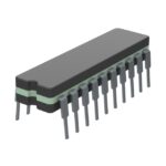 SN54LS244J
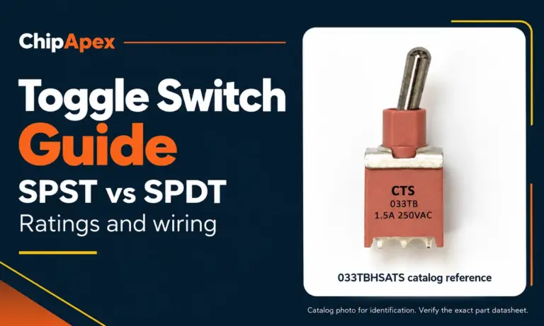
Compare SPST and SPDT toggle switches, understand AC/DC ratings, and follow wiring examples. Check contact action, mounting and parts in the ChipApex catalog.
Read More
SN54LS244J is listed in the Buffers, Drivers, Receivers, Transceivers range at ChipApex. The manufacturer field lists Texas Instruments. Its product description is MILITARY 8-CH,…
Read More
Find out when a bare shock switch needs a pull resistor, when an MCU internal pull-up is enough, and why sensor modules and piezo…
Read More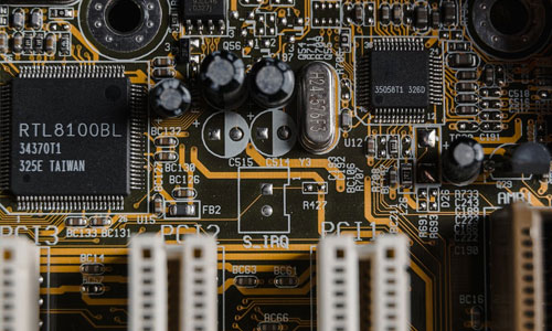
SN54LS244J is listed in the Buffers, Drivers, Receivers, Transceivers range at ChipApex. The manufacturer field lists Texas Instruments. Its product description is MILITARY 8-CH,…
Read More
SN54LS244J is listed in the Buffers, Drivers, Receivers, Transceivers range at ChipApex. The manufacturer field lists Texas Instruments. Its product description is MILITARY 8-CH,…
Read More
SN54LS244J is listed in the Buffers, Drivers, Receivers, Transceivers range at ChipApex. The manufacturer field lists Texas Instruments. Its product description is MILITARY 8-CH,…
Read More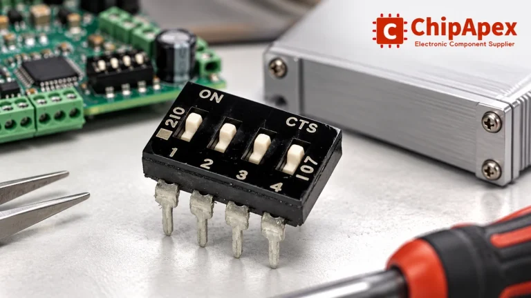
Choose a DIP switch by contact type, coded positions, footprint and signal ratings. Check logic polarity, assembly conditions and PCB configuration behavior.
Read More
SN54LS244J is listed in the Buffers, Drivers, Receivers, Transceivers range at ChipApex. The manufacturer field lists Texas Instruments. Its product description is MILITARY 8-CH,…
Read More
SN54LS244J is listed in the Buffers, Drivers, Receivers, Transceivers range at ChipApex. The manufacturer field lists Texas Instruments. Its product description is MILITARY 8-CH,…
Read More
SN54LS244J is listed in the Buffers, Drivers, Receivers, Transceivers range at ChipApex. The manufacturer field lists Texas Instruments. Its product description is MILITARY 8-CH,…
Read More
See how a MEMS gyroscope measures angular rate, why its angle estimate drifts, and which range, noise, interface and temperature specs to compare.
Read More
Choose an AC to DC converter by input range, output demand, isolation, efficiency and thermal derating. Compare architectures and check installation needs.
Read More
The activity of extra discounts on wholesale prices is in full swing…
Please fill in your contact information and we will send you the latest wholesale price list.





