 ChipApex | Global Electronic Components Supplier

SEARCH
Search Product
Search Post
— IC芯片 | 连接器 | 传感器 | 被动器件 —
Search productSearch post
— IC芯片 | 连接器 | 传感器 | 被动器件 —
Consult the customer manager about the wholesale price.
consultation hotline:86-132-6715-2157
email:[email protected]
Contact the product manager for consultation. One-stop consultation is available.
Do you want a lower wholesale price? Please send us your inquiry and we will reply immediately.
SN74ABT16853DLR is listed in the Buffers, Drivers, Receivers, Transceivers range at ChipApex. The manufacturer field lists Texas Instruments. Its product description is IC TXRX NON-INVERT 5.5V 56SSOP. Review the specifications below when checking this part for your BOM.
The SN74ABT16853DLR is a dual 8-bit to 9-bit parity bus transceiver utilizing Texas Instruments' EPIC-IIB BiCMOS technology. It operates within a supply voltage range of 4.5 V to 5.5 V and supports an operating temperature range from -40°C to +85°C. The device features high-drive outputs capable of sourcing -32 mA and sinking 64 mA, with typical propagation delays ranging from 1.5 ns to 7.7 ns depending on the signal path. It incorporates distributed VCC and GND pin configurations to minimize switching noise.
Verify the specific DL suffix indicates the plastic shrink small-outline package configuration. Confirm that the component meets the commercial temperature specifications of -40°C to +85°C rather than military grades. Ensure design compliance with absolute maximum ratings regarding input clamp currents and output short-circuit conditions during integration.
Select this component when dual independent 8-bit bidirectional transfer with built-in odd/even parity generation is required. The flow-through architecture facilitates efficient board routing compared to wrap-around designs. Consider the high-drive capability for driving multiple loads or longer traces without external buffering.
This part belongs to the Widebus family of logic devices designed by Texas Instruments. It utilizes EPIC-IIB BiCMOS technology to achieve significantly reduced power dissipation while maintaining high-speed performance. The device provides latch-up protection exceeding 500 mA per JEDEC standards.
SN54ABT16853 (Military grade variant)
When both OEA and OEB are low, data transfers from A to B and generates inverted parity, which acts as a forced error condition to enhance system diagnostic capabilities.
The open-collector ERR output indicates whether a parity error has occurred in the B data when transmitting from B to A. Its state can be passed, sampled, stored, or cleared via LE and CLR inputs.
Explore related parts through Logic, Integrated Circuits (ICs), all product categories, ChipApex homepage.
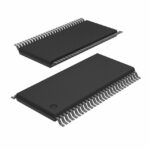 SN74ABT16853DLR
SN74ABT16853DLR is listed in the Buffers, Drivers, Receivers, Transceivers range at ChipApex. The manufacturer field lists Texas Instruments. Its product description is IC TXRX…
Read More
SN74ABT16853DLR is listed in the Buffers, Drivers, Receivers, Transceivers range at ChipApex. The manufacturer field lists Texas Instruments. Its product description is IC TXRX…
Read More
SN74ABT16853DLR is listed in the Buffers, Drivers, Receivers, Transceivers range at ChipApex. The manufacturer field lists Texas Instruments. Its product description is IC TXRX…
Read More
SN74ABT16853DLR is listed in the Buffers, Drivers, Receivers, Transceivers range at ChipApex. The manufacturer field lists Texas Instruments. Its product description is IC TXRX…
Read More
SN74ABT16853DLR is listed in the Buffers, Drivers, Receivers, Transceivers range at ChipApex. The manufacturer field lists Texas Instruments. Its product description is IC TXRX…
Read More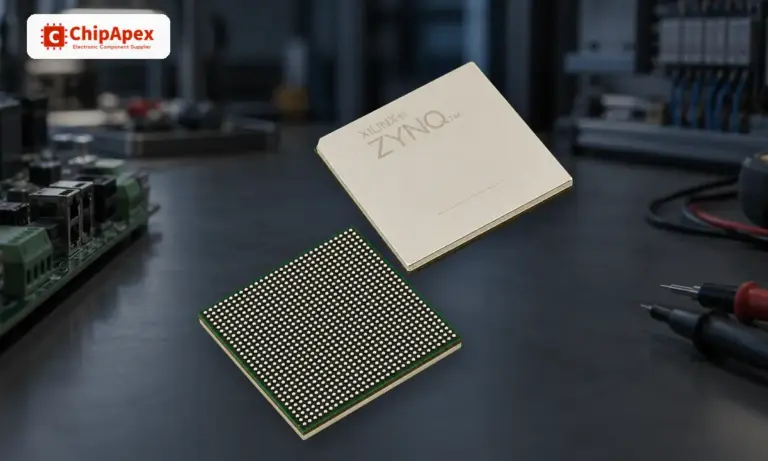
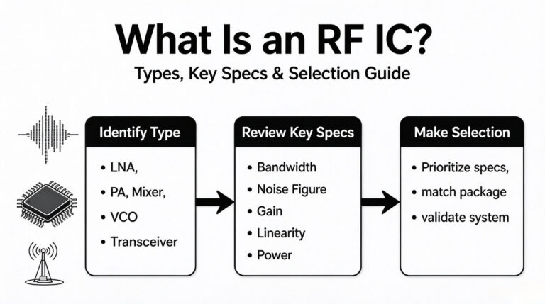
Learn what an integrated circuit is, how ICs work, the main types and the specs to check before choosing a part for your design…
Read More
Choose an AC to DC converter by input range, output demand, isolation, efficiency and thermal derating. Compare architectures and check installation needs.
Read More
SN74ABT16853DLR is listed in the Buffers, Drivers, Receivers, Transceivers range at ChipApex. The manufacturer field lists Texas Instruments. Its product description is IC TXRX…
Read More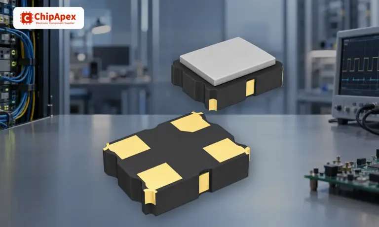
Understand how oscillators generate timing signals, how they differ from crystals, and which frequency, output and stability specs matter when choosing one.
Read More
SN74ABT16853DLR is listed in the Buffers, Drivers, Receivers, Transceivers range at ChipApex. The manufacturer field lists Texas Instruments. Its product description is IC TXRX…
Read More
SN74ABT16853DLR is listed in the Buffers, Drivers, Receivers, Transceivers range at ChipApex. The manufacturer field lists Texas Instruments. Its product description is IC TXRX…
Read More
SN74ABT16853DLR is listed in the Buffers, Drivers, Receivers, Transceivers range at ChipApex. The manufacturer field lists Texas Instruments. Its product description is IC TXRX…
Read More
The activity of extra discounts on wholesale prices is in full swing…
Please fill in your contact information and we will send you the latest wholesale price list.





