 ChipApex | Global Electronic Components Supplier

SEARCH
Search Product
Search Post
— IC芯片 | 连接器 | 传感器 | 被动器件 —
Search productSearch post
— IC芯片 | 连接器 | 传感器 | 被动器件 —
Consult the customer manager about the wholesale price.
consultation hotline:86-132-6715-2157
email:[email protected]
Contact the product manager for consultation. One-stop consultation is available.
Do you want a lower wholesale price? Please send us your inquiry and we will reply immediately.
SN74ABT841ADBRE4 is listed in the Latches range at ChipApex. The manufacturer field lists Texas Instruments. Its product description is IC 10BIT BUS-INTFC D 3ST 24-SSOP. Review the specifications below when checking this part for your BOM.
The SN74ABT841ADBRE4 is a 10-bit bus-interface D-type latch with 3-state outputs manufactured by Texas Instruments. It utilizes EPIC-IIB BiCMOS design for reduced power dissipation and features high-drive outputs capable of -32 mA IOH and 64 mA IOL. The device operates within a supply voltage range of 4.5 V to 5.5 V and supports an operating temperature range from -40°C to +85°C. It includes ESD protection exceeding 2000 V per MIL-STD-883 and latch-up performance exceeding 500 mA per JEDEC JESD-17. The component is housed in a 24-pin SSOP package.
Verify the specific ordering suffix 'E4' corresponds to lead-free (NIPDAU) finish and RoHS compliance as indicated in the packaging data. Confirm the package type matches the DB drawing for SSOP-24 requirements. Ensure the application environment stays within the specified -40°C to +85°C operating temperature range. Check that unused inputs are held high or low to prevent floating states.
Select this component when a 10-bit wide storage interface is required with high drive capability. The ABT series offers faster switching characteristics compared to standard TTL families. Consider the SSOP package dimensions if board space is constrained relative to larger SOIC or DIP options. Verify that the 4.5 V to 5.5 V supply voltage aligns with the system power architecture.
This part belongs to the SN74ABT841A family of 10-bit latches. It shares functional similarities with other ABT logic devices but is distinct in its 10-bit width and specific latch configuration. The 'DB' suffix denotes the Shrink Small-Outline Package, while 'E4' indicates environmental compliance. It serves as a bridge between microprocessors and external memory or peripheral buses.
SN74ABT841ADBR
The OE pin places outputs in a high-impedance state but does not affect the internal operations of the latch. Previously stored data can be retained or new data entered while outputs are disabled.
When VCC is between 0 and 2.1 V, the device enters a high-impedance state automatically. To ensure this state above 2.1 V, OE should be tied to VCC through a pullup resistor.
Explore related parts through Logic, Integrated Circuits (ICs), all product categories, ChipApex homepage.
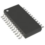 SN74ABT841ADBRE4

SN74ABT841ADBRE4 is listed in the Latches range at ChipApex. The manufacturer field lists Texas Instruments. Its product description is IC 10BIT BUS-INTFC D 3ST…
Read More
SN74ABT841ADBRE4 is listed in the Latches range at ChipApex. The manufacturer field lists Texas Instruments. Its product description is IC 10BIT BUS-INTFC D 3ST…
Read More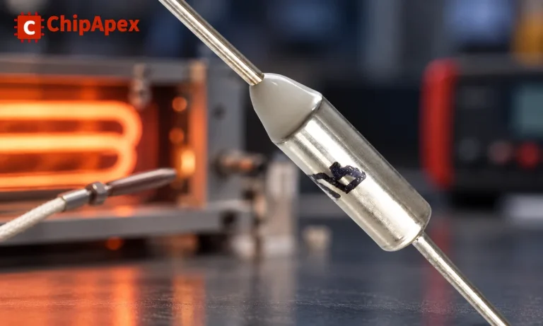
Understand thermal fuse operation, Tf, Th and Tm, electrical ratings and mounting. Check temperature limits and replacement requirements for your design.
Read More
SN74ABT841ADBRE4 is listed in the Latches range at ChipApex. The manufacturer field lists Texas Instruments. Its product description is IC 10BIT BUS-INTFC D 3ST…
Read MoreSN74ABT841ADBRE4 is listed in the Latches range at ChipApex. The manufacturer field lists Texas Instruments. Its product description is IC 10BIT BUS-INTFC D 3ST…
Read More
SN74ABT841ADBRE4 is listed in the Latches range at ChipApex. The manufacturer field lists Texas Instruments. Its product description is IC 10BIT BUS-INTFC D 3ST…
Read More
SN74ABT841ADBRE4 is listed in the Latches range at ChipApex. The manufacturer field lists Texas Instruments. Its product description is IC 10BIT BUS-INTFC D 3ST…
Read More
Select a bridge rectifier by reverse voltage, capacitor charging current, startup surge and cooling. Work through a stated DC voltage and ripple example.
Read More
SN74ABT841ADBRE4 is listed in the Latches range at ChipApex. The manufacturer field lists Texas Instruments. Its product description is IC 10BIT BUS-INTFC D 3ST…
Read More
Compare RC, crystal and MEMS oscillator circuits. Check ppm, jitter, load capacitance, startup margin and output compatibility before choosing a clock source.
Read More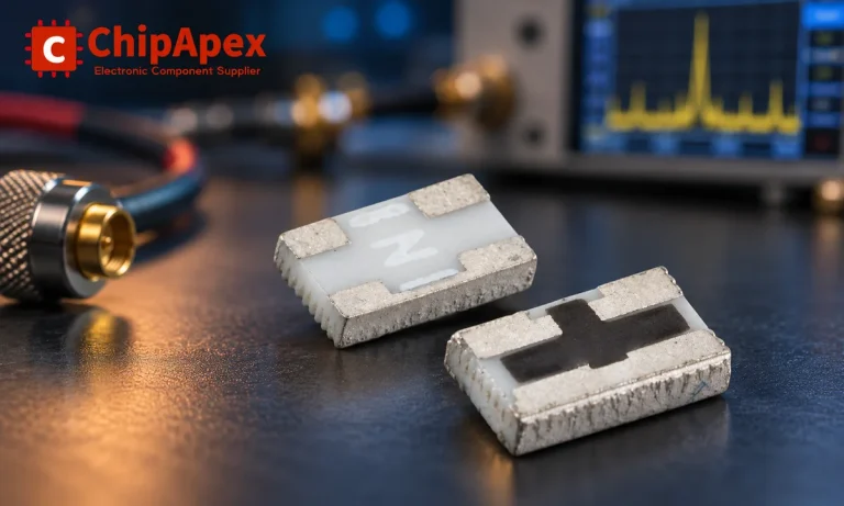
Understand RF attenuator dB values, fixed and programmable types, impedance, power limits and noise tradeoffs before choosing parts for an RF signal path.
Read More
SN74ABT841ADBRE4 is listed in the Latches range at ChipApex. The manufacturer field lists Texas Instruments. Its product description is IC 10BIT BUS-INTFC D 3ST…
Read More
The activity of extra discounts on wholesale prices is in full swing…
Please fill in your contact information and we will send you the latest wholesale price list.





