 ChipApex | Global Electronic Components Supplier

SEARCH
Search Product
Search Post
— IC芯片 | 连接器 | 传感器 | 被动器件 —
Search productSearch post
— IC芯片 | 连接器 | 传感器 | 被动器件 —
Consult the customer manager about the wholesale price.
consultation hotline:86-132-6715-2157
email:[email protected]
Contact the product manager for consultation. One-stop consultation is available.
Do you want a lower wholesale price? Please send us your inquiry and we will reply immediately.
SN74ACT7881-20PN is listed in the FIFOs Memory range at ChipApex. The manufacturer field lists Texas Instruments. Its product description is IC FIFO SYNC 1KX18 13NS 80LQFP. Review the specifications below when checking this part for your BOM.
The SN74ACT7881-20PN is a synchronous first-in, first-out memory device organized as 1024 words by 18 bits. It operates with a supply voltage range of 4.5 V to 5.5 V and supports data rates up to 50 MHz. The component features independent asynchronous inputs and outputs, allowing read and write operations to be synchronized to separate system clocks. It provides fast access times of 13 ns maximum and includes programmable status flags for buffer management.
Verify the specific -20 speed grade suffix against current Texas Instruments documentation to confirm timing parameters. Confirm package integrity for the 80-pin shrink quad flat configuration. Check for obsolescence status and lead-free compliance requirements prior to ordering. Ensure design compatibility with recommended operating conditions.
Select this component when 18-bit word width and 1024-word depth are required. Choose the -20 variant if system timing allows up to 50 MHz operation. Consider the PN package for surface-mount assembly needs. Evaluate expansion capabilities if deeper or wider memory structures are necessary for the application design.
This part belongs to the SN74ACT7881 family of clocked FIFO memories within the Widebus product line. It shares pinout compatibility with related models such as the SN74ACT7882 and SN74ACT7884. The device utilizes ACT logic technology for standard 5-V CMOS operation. It is designed for high-performance data buffering in complex digital architectures.
SN74ACT7881-15FN
The boundary is defined by an offset value (X) programmed during the reset cycle using the DAF pin and data inputs, or it defaults to 256.
These pins must be held high before the rising edge of the write clock to enable writing data into the FIFO memory.
Explore related parts through Logic, Integrated Circuits (ICs), all product categories, ChipApex homepage.
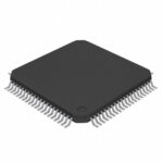 SN74ACT7881-20PN

Select a bridge rectifier by reverse voltage, capacitor charging current, startup surge and cooling. Work through a stated DC voltage and ripple example.
Read More
SN74ACT7881-20PN is listed in the FIFOs Memory range at ChipApex. The manufacturer field lists Texas Instruments. Its product description is IC FIFO SYNC 1KX18…
Read More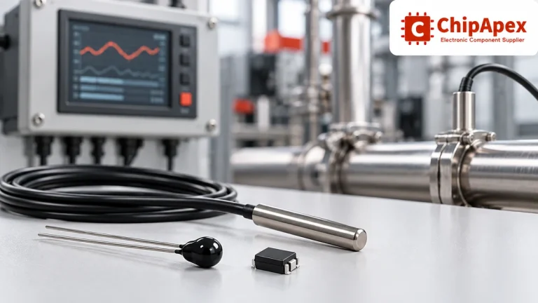
Compare thermistors, RTDs, thermocouples and temperature ICs. Learn how range, accuracy, response, interfaces and mounting affect component selection.
Read More
SN74ACT7881-20PN is listed in the FIFOs Memory range at ChipApex. The manufacturer field lists Texas Instruments. Its product description is IC FIFO SYNC 1KX18…
Read More
SN74ACT7881-20PN is listed in the FIFOs Memory range at ChipApex. The manufacturer field lists Texas Instruments. Its product description is IC FIFO SYNC 1KX18…
Read More
SN74ACT7881-20PN is listed in the FIFOs Memory range at ChipApex. The manufacturer field lists Texas Instruments. Its product description is IC FIFO SYNC 1KX18…
Read More
SN74ACT7881-20PN is listed in the FIFOs Memory range at ChipApex. The manufacturer field lists Texas Instruments. Its product description is IC FIFO SYNC 1KX18…
Read More
SN74ACT7881-20PN is listed in the FIFOs Memory range at ChipApex. The manufacturer field lists Texas Instruments. Its product description is IC FIFO SYNC 1KX18…
Read More
SN74ACT7881-20PN is listed in the FIFOs Memory range at ChipApex. The manufacturer field lists Texas Instruments. Its product description is IC FIFO SYNC 1KX18…
Read More
Choose an AC to DC converter by input range, output demand, isolation, efficiency and thermal derating. Compare architectures and check installation needs.
Read More
SN74ACT7881-20PN is listed in the FIFOs Memory range at ChipApex. The manufacturer field lists Texas Instruments. Its product description is IC FIFO SYNC 1KX18…
Read More
SN74ACT7881-20PN is listed in the FIFOs Memory range at ChipApex. The manufacturer field lists Texas Instruments. Its product description is IC FIFO SYNC 1KX18…
Read More
The activity of extra discounts on wholesale prices is in full swing…
Please fill in your contact information and we will send you the latest wholesale price list.





