 ChipApex | Global Electronic Components Supplier

SEARCH
Search Product
Search Post
— IC芯片 | 连接器 | 传感器 | 被动器件 —
Search productSearch post
— IC芯片 | 连接器 | 传感器 | 被动器件 —
Consult the customer manager about the wholesale price.
consultation hotline:86-132-6715-2157
email:[email protected]
Contact the product manager for consultation. One-stop consultation is available.
Do you want a lower wholesale price? Please send us your inquiry and we will reply immediately.
SN74ALVC125PWE4 is listed in the Buffers, Drivers, Receivers, Transceivers range at ChipApex. The manufacturer field lists Texas Instruments. Its product description is IC BUF NON-INVERT 3.6V 14TSSOP. Review the specifications below when checking this part for your BOM.
The SN74ALVC125PWE4 is a quadruple bus buffer gate with 3-state outputs manufactured by Texas Instruments. It operates from a supply voltage range of 1.65 V to 3.6 V and features independent line drivers. The device provides an output drive capability of ±24 mA at 3.6 V. Each output is disabled when the associated output-enable (OE) input is high. The component is housed in a 14-pin TSSOP package and supports an operating free-air temperature range of -40 °C to 85 °C.
Verify that the ordering suffix 'E4' corresponds to the specific lead finish and RoHS compliance requirements mandated by your assembly process. Confirm the package type matches the PCB footprint design, as the PW designation indicates a TSSOP housing. Ensure the selected variant aligns with the required thermal impedance and moisture sensitivity level ratings for your manufacturing environment.
Select this component when designing systems that require low-power logic operation within the 1.65 V to 3.6 V supply range. It is suitable for applications needing high-speed signal buffering with propagation delays as low as 2.8 ns at 3.3 V. Consider the ±24 mA output drive capability for driving moderate capacitive loads on system buses without external amplification.
This part belongs to the ALVC logic family, which is designed for low-voltage CMOS applications. It serves as a quadruple bus buffer gate, providing three-state outputs controlled by individual enable inputs. The device is intended for use in portable and battery-operated equipment where power consumption is a critical design constraint.
SN74ALVC125PW
Each output is disabled and enters a high-impedance state when the associated output-enable (OE) input is high.
The maximum propagation delay (t_pd) is 2.8 ns when operating at a supply voltage of 3.3 V.
Explore related parts through Logic, Integrated Circuits (ICs), all product categories, ChipApex homepage.
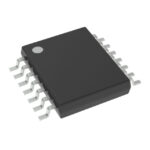 SN74ALVC125PWE4
SN74ALVC125PWE4 is listed in the Buffers, Drivers, Receivers, Transceivers range at ChipApex. The manufacturer field lists Texas Instruments. Its product description is IC BUF…
Read More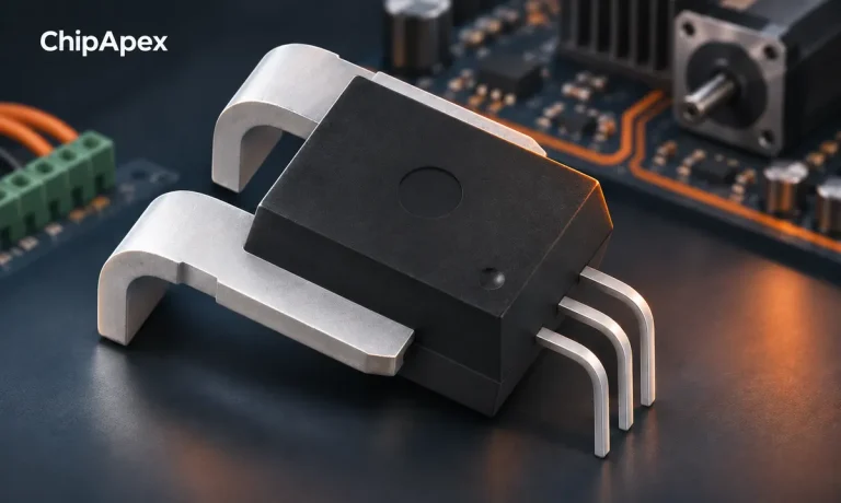
Compare Hall, shunt, current transformer and Rogowski sensing. Check AC/DC capability, accuracy, isolation, heat and response before selecting a sensor.
Read More
SN74ALVC125PWE4 is listed in the Buffers, Drivers, Receivers, Transceivers range at ChipApex. The manufacturer field lists Texas Instruments. Its product description is IC BUF…
Read More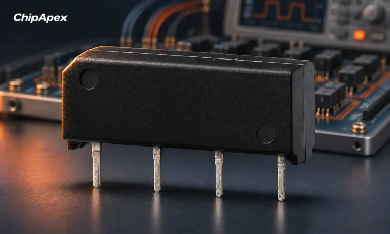
Choose a reed relay for signal switching. Understand hot and cold switching, leakage, contact resistance, isolation and measurement settling requirements.
Read More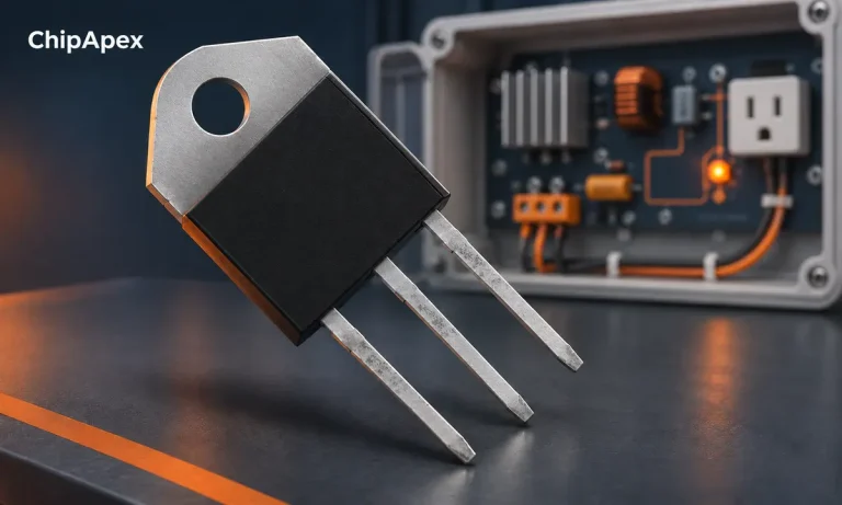
Learn how a TRIAC switches AC loads. Understand triggering, latching, holding current, phase control and thermal limits before choosing a component.
Read More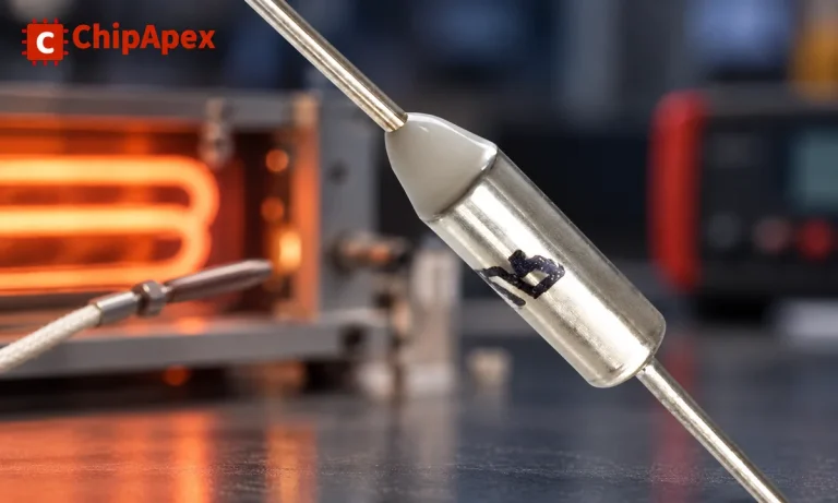
Understand thermal fuse operation, Tf, Th and Tm, electrical ratings and mounting. Check temperature limits and replacement requirements for your design.
Read More
SN74ALVC125PWE4 is listed in the Buffers, Drivers, Receivers, Transceivers range at ChipApex. The manufacturer field lists Texas Instruments. Its product description is IC BUF…
Read More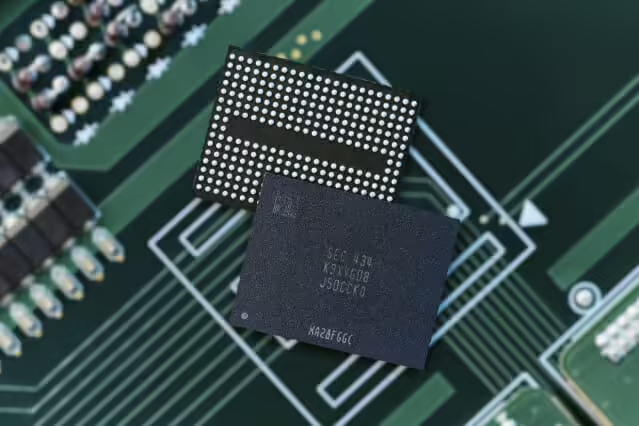
SN74ALVC125PWE4 is listed in the Buffers, Drivers, Receivers, Transceivers range at ChipApex. The manufacturer field lists Texas Instruments. Its product description is IC BUF…
Read More
SN74ALVC125PWE4 is listed in the Buffers, Drivers, Receivers, Transceivers range at ChipApex. The manufacturer field lists Texas Instruments. Its product description is IC BUF…
Read More
Learn how a JFET works and how to compare bias, leakage, noise and pinout. Review practical selection questions for high-impedance analog circuits.
Read More
Choose a vibration sensor for machine monitoring. Compare sensing methods, bandwidth, noise and mounting, then define the signal-chain requirements.
Read More
SN74ALVC125PWE4 is listed in the Buffers, Drivers, Receivers, Transceivers range at ChipApex. The manufacturer field lists Texas Instruments. Its product description is IC BUF…
Read More
The activity of extra discounts on wholesale prices is in full swing…
Please fill in your contact information and we will send you the latest wholesale price list.





