 ChipApex | Global Electronic Components Supplier

SEARCH
Search Product
Search Post
— IC芯片 | 连接器 | 传感器 | 被动器件 —
Search productSearch post
— IC芯片 | 连接器 | 传感器 | 被动器件 —
Consult the customer manager about the wholesale price.
consultation hotline:86-132-6715-2157
email:[email protected]
Contact the product manager for consultation. One-stop consultation is available.
Do you want a lower wholesale price? Please send us your inquiry and we will reply immediately.
SN74ALVCH16344DLR is listed in the Buffers, Drivers, Receivers, Transceivers range at ChipApex. The manufacturer field lists Texas Instruments. Its product description is IC ADDRESS DRIVER 3.6V 56SSOP. Review the specifications below when checking this part for your BOM.
The SN74ALVCH16344DLR is a 1-bit to 4-bit address driver with 3-state outputs, designed for 1.65-V to 3.6-V VCC operation. It contains four separate drivers, each converting one input to four outputs. The device features active bus-hold circuitry on data inputs to eliminate the need for external pullup or pulldown resistors. It operates within an ambient temperature range of -40°C to 85°C and is housed in a 56-pin SSOP (DL) package.
Verify component authenticity as this part is obsolete. Confirm that the DL suffix corresponds to the SSOP package type. Ensure the replacement meets the required voltage and temperature specifications if sourcing from secondary markets.
Select this component when designing systems requiring a single address signal to drive multiple memory banks simultaneously. Verify compatibility with the target supply voltage range between 1.65 V and 3.6 V. Consider the 56-pin SSOP footprint constraints during PCB layout planning.
This device belongs to the Texas Instruments Widebus family of logic components. It functions specifically as an address driver rather than a standard buffer or transceiver. The DL suffix indicates the plastic small-outline package variant manufactured by Texas Instruments.
SN74ALVCH16344DL is listed as a direct substitute.
Active bus-hold circuitry holds unused or undriven inputs at a valid logic state, removing the requirement for external pullup or pulldown resistors.
Tying the Output Enable (OE) pin to VCC through a pullup resistor ensures a high-impedance state during power up or power down conditions.
Explore related parts through Logic, Integrated Circuits (ICs), all product categories, ChipApex homepage.
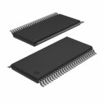 SN74ALVCH16344DLR
Choose LED drivers by current, string voltage, dimming and thermal limits. Understand constant-current operation and the checks needed for your load.
Read More
SN74ALVCH16344DLR is listed in the Buffers, Drivers, Receivers, Transceivers range at ChipApex. The manufacturer field lists Texas Instruments. Its product description is IC ADDRESS…
Read More
SN74ALVCH16344DLR is listed in the Buffers, Drivers, Receivers, Transceivers range at ChipApex. The manufacturer field lists Texas Instruments. Its product description is IC ADDRESS…
Read More
SN74ALVCH16344DLR is listed in the Buffers, Drivers, Receivers, Transceivers range at ChipApex. The manufacturer field lists Texas Instruments. Its product description is IC ADDRESS…
Read More
Understand automotive relay terminals, coil suppression and load ratings. Check inrush, socket compatibility and temperature before selecting a replacement.
Read More
SN74ALVCH16344DLR is listed in the Buffers, Drivers, Receivers, Transceivers range at ChipApex. The manufacturer field lists Texas Instruments. Its product description is IC ADDRESS…
Read More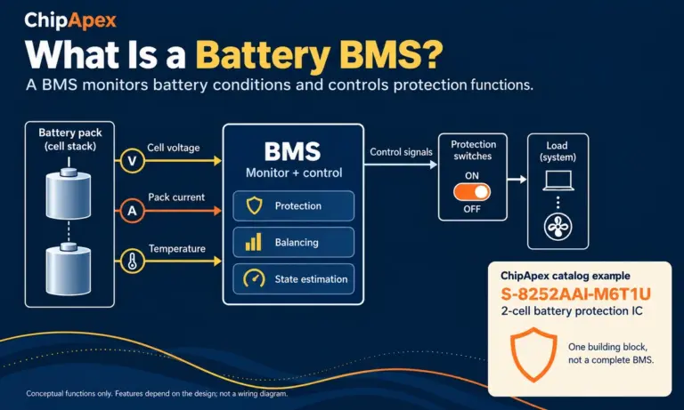
Learn what a battery BMS does, how protection differs from charging, and which pack specifications to check when sourcing BMS components through ChipApex.
Read More
SN74ALVCH16344DLR is listed in the Buffers, Drivers, Receivers, Transceivers range at ChipApex. The manufacturer field lists Texas Instruments. Its product description is IC ADDRESS…
Read More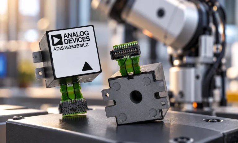
Learn what an IMU measures, how accelerometers and gyroscopes work together, why orientation estimates drift, and what to compare.
Read More
SN74ALVCH16344DLR is listed in the Buffers, Drivers, Receivers, Transceivers range at ChipApex. The manufacturer field lists Texas Instruments. Its product description is IC ADDRESS…
Read More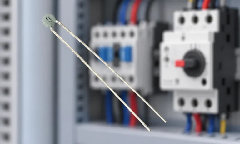
Learn why PTC resistance rises with temperature, how it differs from NTC, and which ratings matter for sensing and protection.
Read More
Learn how a diode conducts, how to identify anode and cathode, and when to choose rectifier, TVS, Zener or photodiode types for a circuit.
Read More
The activity of extra discounts on wholesale prices is in full swing…
Please fill in your contact information and we will send you the latest wholesale price list.





