 ChipApex | Global Electronic Components Supplier

SEARCH
Search Product
Search Post
— IC芯片 | 连接器 | 传感器 | 被动器件 —
Search productSearch post
— IC芯片 | 连接器 | 传感器 | 被动器件 —
Consult the customer manager about the wholesale price.
consultation hotline:86-132-6715-2157
email:[email protected]
Contact the product manager for consultation. One-stop consultation is available.
Do you want a lower wholesale price? Please send us your inquiry and we will reply immediately.
SN74AUC1G125YZTR is listed in the Buffers, Drivers, Receivers, Transceivers range at ChipApex. The manufacturer field lists Texas Instruments. Its product description is IC BUFFER NON-INVERT 2.7V 5DSBGA. Review the specifications below when checking this part for your BOM.
The SN74AUC1G125YZTR is a single bus buffer gate with a 3-state output from the AUC logic family. It operates within a supply voltage range of 0.8 V to 2.7 V and is optimized for 1.65 V to 1.95 V operation. The device features over-voltage tolerant I/Os supporting up to 3.6 V independent of VCC. It provides ±8-mA output drive at 1.8 V with a maximum propagation delay of 2.5 ns at 1.8 V under a 30 pF load. The component utilizes the NanoFree DSBGA package.
Verify the specific YZP (DSBGA, 5) package configuration matches the design footprint requirements. Confirm that the operating temperature range of -40°C to +85°C aligns with the system environment. Ensure input pins are terminated properly to prevent floating states during operation.
Select this component when low voltage operation between 0.8 V and 2.7 V is required. It is suitable for designs needing over-voltage tolerant inputs up to 3.6 V. Consider its small form factor and low power consumption for space-constrained portable electronics.
This device belongs to the Texas Instruments AUC logic family, which is specifically engineered for speed and low power consumption. The AUC series supports sub-1-V little logic operations and is designed to maintain signal integrity while minimizing switching noise in high-frequency digital circuits.
SN74AUC1G125DBVR
The Ioff circuitry disables all outputs when the supply pin is held at 0 V, preventing damaging current backflow through the device during partial power-down conditions.
Unused inputs must not be left floating; they should be tied to VCC or GND to ensure proper device operation and prevent undefined operational states.
Explore related parts through Logic, Integrated Circuits (ICs), all product categories, ChipApex homepage.
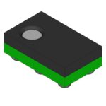 SN74AUC1G125YZTR
SN74AUC1G125YZTR is listed in the Buffers, Drivers, Receivers, Transceivers range at ChipApex. The manufacturer field lists Texas Instruments. Its product description is IC BUFFER…
Read More
SN74AUC1G125YZTR is listed in the Buffers, Drivers, Receivers, Transceivers range at ChipApex. The manufacturer field lists Texas Instruments. Its product description is IC BUFFER…
Read More
Choose an AC to DC converter by input range, output demand, isolation, efficiency and thermal derating. Compare architectures and check installation needs.
Read More
SN74AUC1G125YZTR is listed in the Buffers, Drivers, Receivers, Transceivers range at ChipApex. The manufacturer field lists Texas Instruments. Its product description is IC BUFFER…
Read More
SN74AUC1G125YZTR is listed in the Buffers, Drivers, Receivers, Transceivers range at ChipApex. The manufacturer field lists Texas Instruments. Its product description is IC BUFFER…
Read More
SN74AUC1G125YZTR is listed in the Buffers, Drivers, Receivers, Transceivers range at ChipApex. The manufacturer field lists Texas Instruments. Its product description is IC BUFFER…
Read More
SN74AUC1G125YZTR is listed in the Buffers, Drivers, Receivers, Transceivers range at ChipApex. The manufacturer field lists Texas Instruments. Its product description is IC BUFFER…
Read More
SN74AUC1G125YZTR is listed in the Buffers, Drivers, Receivers, Transceivers range at ChipApex. The manufacturer field lists Texas Instruments. Its product description is IC BUFFER…
Read More
SN74AUC1G125YZTR is listed in the Buffers, Drivers, Receivers, Transceivers range at ChipApex. The manufacturer field lists Texas Instruments. Its product description is IC BUFFER…
Read More
SN74AUC1G125YZTR is listed in the Buffers, Drivers, Receivers, Transceivers range at ChipApex. The manufacturer field lists Texas Instruments. Its product description is IC BUFFER…
Read More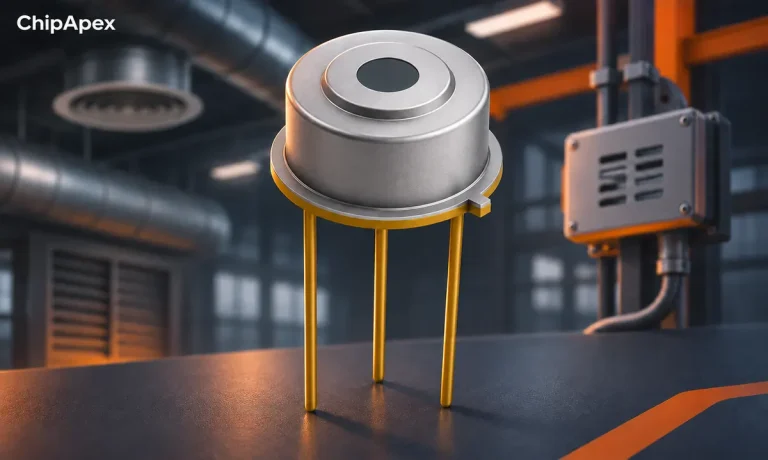
Compare gas sensor technologies, cross-sensitivity and calibration needs. Define the gas, range and environment before choosing a sensing component.
Read More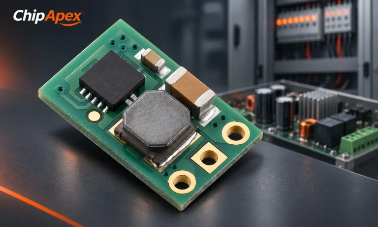
Select a DC-DC converter by input range, topology, isolation and temperature. Compare ripple, efficiency and load limits before choosing a component.
Read More
The activity of extra discounts on wholesale prices is in full swing…
Please fill in your contact information and we will send you the latest wholesale price list.





