 ChipApex | Global Electronic Components Supplier

SEARCH
Search Product
Search Post
— IC芯片 | 连接器 | 传感器 | 被动器件 —
Search productSearch post
— IC芯片 | 连接器 | 传感器 | 被动器件 —
Consult the customer manager about the wholesale price.
consultation hotline:86-132-6715-2157
email:[email protected]
Contact the product manager for consultation. One-stop consultation is available.
Do you want a lower wholesale price? Please send us your inquiry and we will reply immediately.
SN74AVCH16T245VR is listed in the Buffers, Drivers, Receivers, Transceivers range at ChipApex. The manufacturer field lists Texas Instruments. Its product description is IC TRANSLATOR BIDIR 48TVSOP. Review the specifications below when checking this part for your BOM.
The SN74AVCH16T245 is a 16-bit dual-supply noninverting bus transceiver with configurable level-shifting and tri-state outputs. It supports VCCA and VCCB supply voltages ranging from 1.2 V to 3.6 V, enabling universal bidirectional translation between any low-voltage nodes including 1.2 V, 1.5 V, 1.8 V, 2.5 V, and 3.3 V. The device features overvoltage-tolerant I/Os up to 4.6 V, active bus-hold circuitry, and an Ioff circuit for partial-power-down mode. Maximum data rates reach 380 Mbps at 1.8 V to 3.3 V levels.
Verify the specific package suffix (VR indicates TVSOP-48) against the required footprint. Confirm RoHS compliance status as some variants may differ. Ensure ESD handling protocols are followed given the sensitivity of CMOS logic. Cross-reference the datasheet revision date to ensure alignment with current manufacturing specifications.
Select this component when asynchronous communication between buses operating at different voltage levels is required. The dual-supply architecture accommodates varying logic families. Consider the propagation delay characteristics relative to the target clock frequency and load capacitance. Verify that the control pins are driven by the VCCA rail for proper functionality.
This device belongs to the Texas Instruments SN74AVCH series of advanced CMOS logic. It is designed specifically for high-speed data transmission in environments requiring flexible voltage translation. The 16-bit width reduces board space compared to using multiple 8-bit transceivers. It serves as a bridge between legacy and modern low-voltage digital systems.
Check for pin-compatible alternatives within the same logic family if package availability is constrained. Ensure substitute parts maintain the 1.2 V to 3.6 V operating range and similar propagation delays. Verify that any replacement also supports the required Ioff and VCC isolation features for system safety.
If either VCCA or VCCB input is at GND, both ports enter a high-impedance state. This prevents false logic levels from appearing on either bus during power sequencing or fault conditions.
The Ioff circuit disables the outputs to prevent damaging current backflow through the device when it is in a partial-power-down mode. This ensures safe operation when one side of the bus is powered while the other is not.
Explore related parts through Logic, Integrated Circuits (ICs), all product categories, ChipApex homepage.
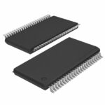 SN74AVCH16T245VR

SN74AVCH16T245VR is listed in the Buffers, Drivers, Receivers, Transceivers range at ChipApex. The manufacturer field lists Texas Instruments. Its product description is IC TRANSLATOR…
Read More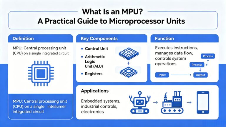
SN74AVCH16T245VR is listed in the Buffers, Drivers, Receivers, Transceivers range at ChipApex. The manufacturer field lists Texas Instruments. Its product description is IC TRANSLATOR…
Read More
SN74AVCH16T245VR is listed in the Buffers, Drivers, Receivers, Transceivers range at ChipApex. The manufacturer field lists Texas Instruments. Its product description is IC TRANSLATOR…
Read More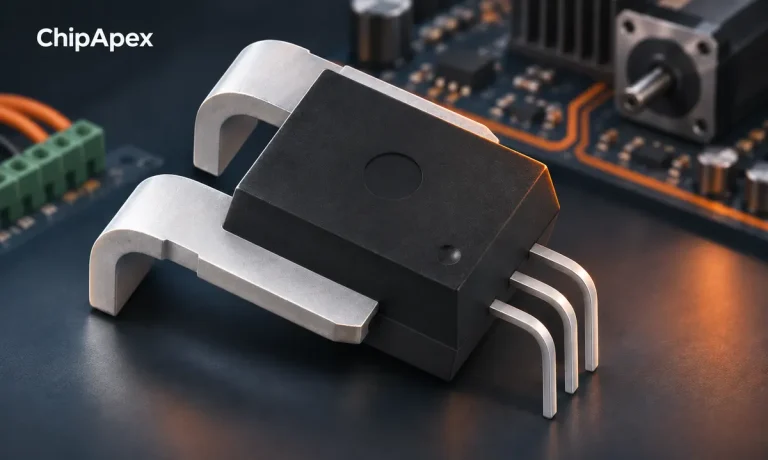
Compare Hall, shunt, current transformer and Rogowski sensing. Check AC/DC capability, accuracy, isolation, heat and response before selecting a sensor.
Read More
SN74AVCH16T245VR is listed in the Buffers, Drivers, Receivers, Transceivers range at ChipApex. The manufacturer field lists Texas Instruments. Its product description is IC TRANSLATOR…
Read More
Choose LED drivers by current, string voltage, dimming and thermal limits. Understand constant-current operation and the checks needed for your load.
Read More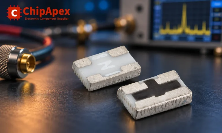
Understand RF attenuator dB values, fixed and programmable types, impedance, power limits and noise tradeoffs before choosing parts for an RF signal path.
Read More
SN74AVCH16T245VR is listed in the Buffers, Drivers, Receivers, Transceivers range at ChipApex. The manufacturer field lists Texas Instruments. Its product description is IC TRANSLATOR…
Read More
SN74AVCH16T245VR is listed in the Buffers, Drivers, Receivers, Transceivers range at ChipApex. The manufacturer field lists Texas Instruments. Its product description is IC TRANSLATOR…
Read More
SN74AVCH16T245VR is listed in the Buffers, Drivers, Receivers, Transceivers range at ChipApex. The manufacturer field lists Texas Instruments. Its product description is IC TRANSLATOR…
Read More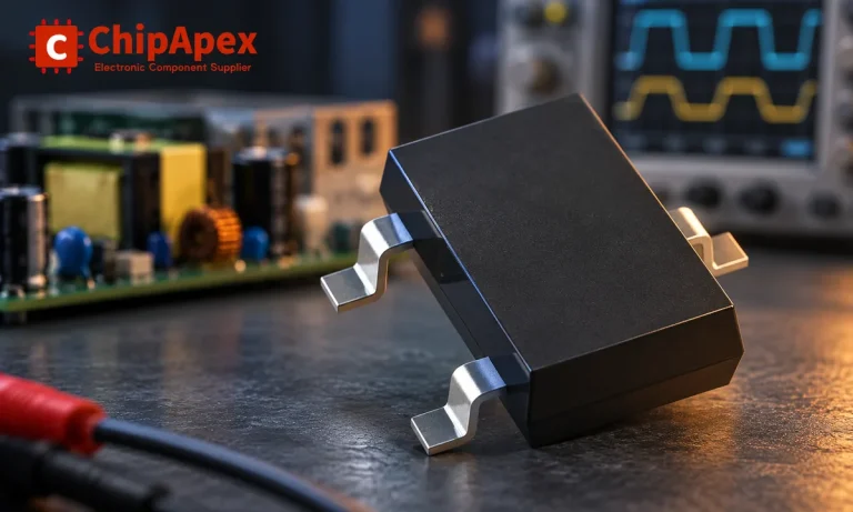
Learn how rectifiers convert AC to DC, compare half-wave and bridge circuits, and select voltage, current, recovery and thermal ratings for your design.
Read More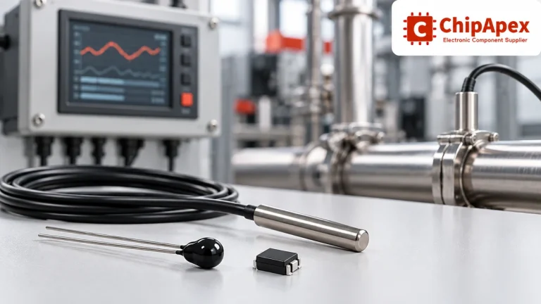
Compare thermistors, RTDs, thermocouples and temperature ICs. Learn how range, accuracy, response, interfaces and mounting affect component selection.
Read More
The activity of extra discounts on wholesale prices is in full swing…
Please fill in your contact information and we will send you the latest wholesale price list.





