 ChipApex | Global Electronic Components Supplier

SEARCH
Search Product
Search Post
— IC芯片 | 连接器 | 传感器 | 被动器件 —
Search productSearch post
— IC芯片 | 连接器 | 传感器 | 被动器件 —
Consult the customer manager about the wholesale price.
consultation hotline:86-132-6715-2157
email:[email protected]
Contact the product manager for consultation. One-stop consultation is available.
Do you want a lower wholesale price? Please send us your inquiry and we will reply immediately.
SN74HC244DWG4 is listed in the Buffers, Drivers, Receivers, Transceivers range at ChipApex. The manufacturer field lists Texas Instruments. Its product description is IC BUFFER NON-INVERT 6V 20SOIC. Review the specifications below when checking this part for your BOM.
The SN74HC244DWG4 is an octal buffer and line driver featuring 3-state outputs, manufactured by Texas Instruments. It operates within a supply voltage range of 2V to 6V and supports a maximum operating temperature of 125°C. The device provides high-current outputs capable of driving up to 15 LSTTL loads, with typical propagation delays ranging from 11ns to 165ns depending on voltage and load conditions. It utilizes standard CMOS inputs and consumes low power, with a maximum ICC of 80µA at 25°C.
Verify the specific package type and thermal characteristics against your design requirements before procurement. Confirm that the component meets all necessary environmental standards for your intended application. Ensure proper handling procedures are followed due to electrostatic discharge sensitivity. Review the latest datasheet revisions for any updates to electrical specifications or recommended operating conditions.
Select this component when designing systems requiring octal buffering with 3-state control capabilities. Consider the wide operating voltage range and high drive strength for compatibility with various logic families. Evaluate the thermal performance and packaging options to ensure suitability for your PCB layout constraints and operating environment.
This part belongs to the SNx4HC244 family of octal buffers and line drivers with 3-state outputs. It is designed to improve performance and density in 3-state memory address drivers, clock drivers, and bus-oriented receivers and transmitters. The device consists of two 4-bit buffers with separate output-enable inputs.
SN74HC244DW
Unused inputs must be terminated at VCC or GND to prevent excessive power consumption and potential oscillations.
The Output Enable (OE) pins control the state of the outputs. When low, the outputs are enabled; when high, they enter a high-impedance state.
Explore related parts through Logic, Integrated Circuits (ICs), all product categories, ChipApex homepage.
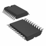 SN74HC244DWG4

SN74HC244DWG4 is listed in the Buffers, Drivers, Receivers, Transceivers range at ChipApex. The manufacturer field lists Texas Instruments. Its product description is IC BUFFER…
Read More
SN74HC244DWG4 is listed in the Buffers, Drivers, Receivers, Transceivers range at ChipApex. The manufacturer field lists Texas Instruments. Its product description is IC BUFFER…
Read More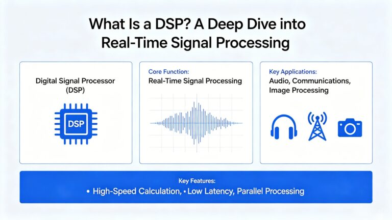
SN74HC244DWG4 is listed in the Buffers, Drivers, Receivers, Transceivers range at ChipApex. The manufacturer field lists Texas Instruments. Its product description is IC BUFFER…
Read More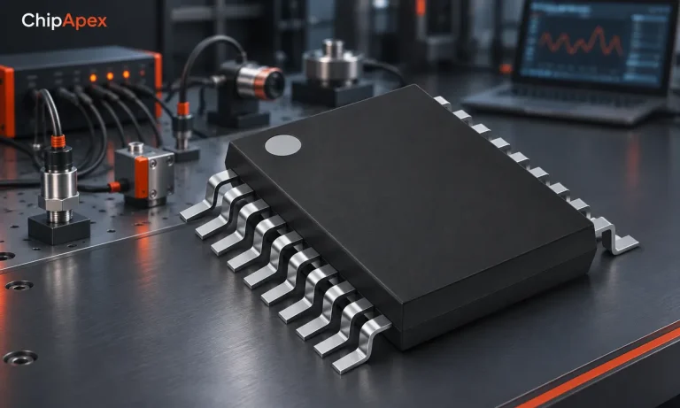
Learn what data acquisition means, from sensors and conditioning to sampling and storage. Review channel timing, wiring, calibration and data quality.
Read More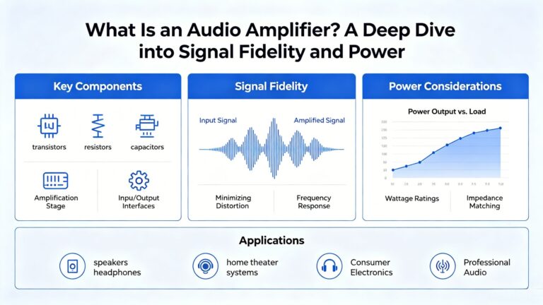
SN74HC244DWG4 is listed in the Buffers, Drivers, Receivers, Transceivers range at ChipApex. The manufacturer field lists Texas Instruments. Its product description is IC BUFFER…
Read More
SN74HC244DWG4 is listed in the Buffers, Drivers, Receivers, Transceivers range at ChipApex. The manufacturer field lists Texas Instruments. Its product description is IC BUFFER…
Read More
SN74HC244DWG4 is listed in the Buffers, Drivers, Receivers, Transceivers range at ChipApex. The manufacturer field lists Texas Instruments. Its product description is IC BUFFER…
Read More
SN74HC244DWG4 is listed in the Buffers, Drivers, Receivers, Transceivers range at ChipApex. The manufacturer field lists Texas Instruments. Its product description is IC BUFFER…
Read More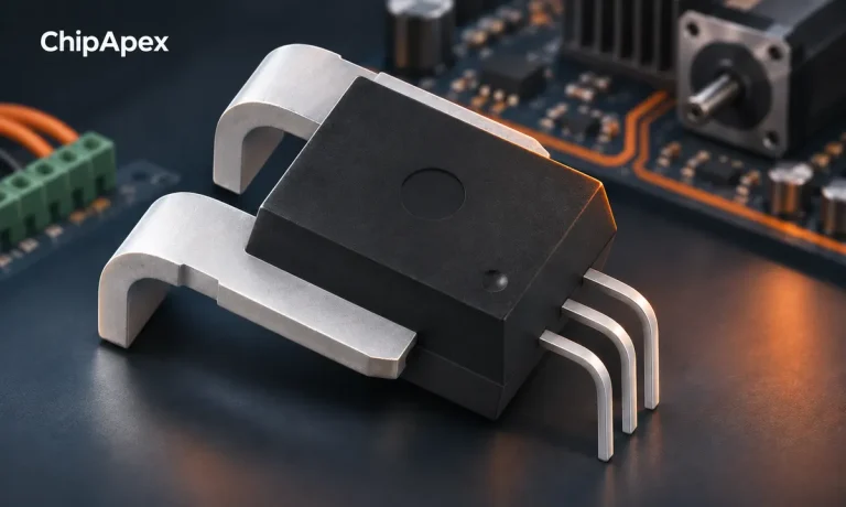
Compare Hall, shunt, current transformer and Rogowski sensing. Check AC/DC capability, accuracy, isolation, heat and response before selecting a sensor.
Read More
SN74HC244DWG4 is listed in the Buffers, Drivers, Receivers, Transceivers range at ChipApex. The manufacturer field lists Texas Instruments. Its product description is IC BUFFER…
Read More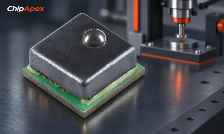
Understand load cell sensor output, bridge wiring and calibration. Learn how mV/V sensitivity, mechanics and ADC noise affect measurement accuracy.
Read More
SN74HC244DWG4 is listed in the Buffers, Drivers, Receivers, Transceivers range at ChipApex. The manufacturer field lists Texas Instruments. Its product description is IC BUFFER…
Read More
The activity of extra discounts on wholesale prices is in full swing…
Please fill in your contact information and we will send you the latest wholesale price list.





