 ChipApex | Global Electronic Components Supplier

SEARCH
Search Product
Search Post
— IC芯片 | 连接器 | 传感器 | 被动器件 —
Search productSearch post
— IC芯片 | 连接器 | 传感器 | 被动器件 —
Consult the customer manager about the wholesale price.
consultation hotline:86-132-6715-2157
email:[email protected]
Contact the product manager for consultation. One-stop consultation is available.
Do you want a lower wholesale price? Please send us your inquiry and we will reply immediately.
SN74HC244PWE4 is listed in the Buffers, Drivers, Receivers, Transceivers range at ChipApex. The manufacturer field lists Texas Instruments. Its product description is IC BUFFER NON-INVERT 6V 20TSSOP. Review the specifications below when checking this part for your BOM.
The SN74HC244PWE4 is an octal buffer and line driver with 3-state outputs manufactured by Texas Instruments. It operates within a supply voltage range of 2V to 6V and supports a maximum operating temperature of 125°C. The device features two independent 4-bit buffers, each controlled by a separate output-enable (OE) input. High-current outputs can drive up to 15 LSTTL loads, while typical propagation delay is 11ns at 5V. Maximum static current consumption is 80µA.
Verify the specific package variant against the datasheet, as the 'PW' suffix indicates TSSOP-20. Confirm that the extended temperature rating of 125°C aligns with system requirements, noting recent revisions may have updated this parameter from previous versions. Ensure ESD handling precautions are followed during installation.
Select this component for applications requiring high-density 3-state memory address drivers or clock drivers. The dual-bank architecture allows flexible signal routing. Verify that the 2V to 6V supply range matches the target logic levels and that the PCB layout accommodates the fast edge rates to minimize ringing on light loads.
This part belongs to the SNx4HC244 family of octal buffers and line drivers. It is designed to improve performance and density in bus-oriented systems. The device utilizes standard CMOS technology, offering balanced output drive and low power consumption compared to older logic families.
Direct replacements include SN74HC244PWR and SN74HC244PWRE4. Other variants such as SN74HC244DWE4 or SN74HC244ANSR offer different packages but share identical electrical characteristics.
Unused inputs must not be left floating. They should be terminated at VCC or GND using a pull-up or pull-down resistor, typically 10kΩ, to ensure proper operation and prevent excessive power consumption.
Each bank of four buffers has a dedicated Output Enable (OE) pin. When OE is low, the buffers pass non-inverted data. When OE is high, the outputs enter a high-impedance state.
Explore related parts through Logic, Integrated Circuits (ICs), all product categories, ChipApex homepage.
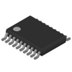 SN74HC244PWE4
Learn what data acquisition means, from sensors and conditioning to sampling and storage. Review channel timing, wiring, calibration and data quality.
Read More
SN74HC244PWE4 is listed in the Buffers, Drivers, Receivers, Transceivers range at ChipApex. The manufacturer field lists Texas Instruments. Its product description is IC BUFFER…
Read More
SN74HC244PWE4 is listed in the Buffers, Drivers, Receivers, Transceivers range at ChipApex. The manufacturer field lists Texas Instruments. Its product description is IC BUFFER…
Read More
SN74HC244PWE4 is listed in the Buffers, Drivers, Receivers, Transceivers range at ChipApex. The manufacturer field lists Texas Instruments. Its product description is IC BUFFER…
Read More
Learn how a TRIAC switches AC loads. Understand triggering, latching, holding current, phase control and thermal limits before choosing a component.
Read More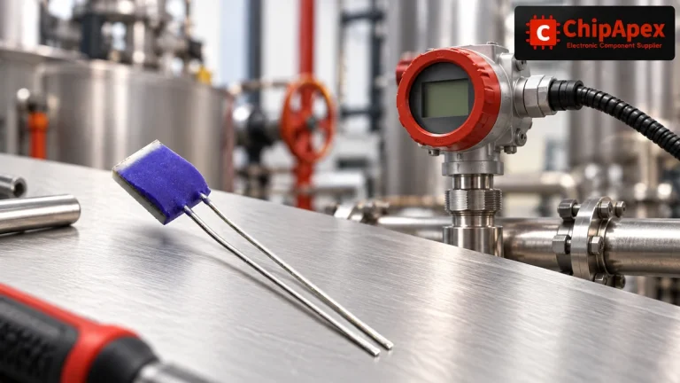
Compare Pt100 and Pt1000 RTDs, two-, three- and four-wire connections, excitation and self-heating. Build an error budget from element to reported temperature.
Read More
SN74HC244PWE4 is listed in the Buffers, Drivers, Receivers, Transceivers range at ChipApex. The manufacturer field lists Texas Instruments. Its product description is IC BUFFER…
Read More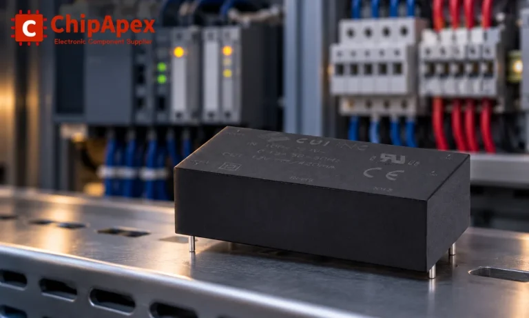
Choose an AC to DC converter by input range, output demand, isolation, efficiency and thermal derating. Compare architectures and check installation needs.
Read More
SN74HC244PWE4 is listed in the Buffers, Drivers, Receivers, Transceivers range at ChipApex. The manufacturer field lists Texas Instruments. Its product description is IC BUFFER…
Read More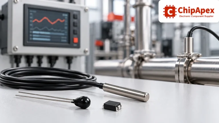
Compare thermistors, RTDs, thermocouples and temperature ICs. Learn how range, accuracy, response, interfaces and mounting affect component selection.
Read MoreSN74HC244PWE4 is listed in the Buffers, Drivers, Receivers, Transceivers range at ChipApex. The manufacturer field lists Texas Instruments. Its product description is IC BUFFER…
Read More
SN74HC244PWE4 is listed in the Buffers, Drivers, Receivers, Transceivers range at ChipApex. The manufacturer field lists Texas Instruments. Its product description is IC BUFFER…
Read More
The activity of extra discounts on wholesale prices is in full swing…
Please fill in your contact information and we will send you the latest wholesale price list.





