 ChipApex | Global Electronic Components Supplier

SEARCH
Search Product
Search Post
— IC芯片 | 连接器 | 传感器 | 被动器件 —
Search productSearch post
— IC芯片 | 连接器 | 传感器 | 被动器件 —
Consult the customer manager about the wholesale price.
consultation hotline:86-132-6715-2157
email:[email protected]
Contact the product manager for consultation. One-stop consultation is available.
Do you want a lower wholesale price? Please send us your inquiry and we will reply immediately.
SN74HCS30QPWRQ1 is listed in the Inverter Gates range at ChipApex. The manufacturer field lists Texas Instruments. Its product description is IC GATE NAND 1CH 8-INP 14TSSOP. Review the specifications below when checking this part for your BOM.
The SN74HCS30QPWRQ1 is an automotive-grade single 8-input NAND gate with Schmitt-trigger inputs manufactured by Texas Instruments. It operates within a supply voltage range of 2 V to 6 V and supports an ambient temperature range from -40°C to +125°C. The device features balanced CMOS push-pull outputs capable of ±7.8 mA drive current at 5 V. Propagation delay ranges from 8 ns to 46 ns depending on the supply voltage. It is housed in a 14-pin TSSOP package.
Verify the specific ordering suffix 'PWRQ1' corresponds to the TSSOP-14 package variant when sourcing. Confirm that the component meets AEC-Q100 Grade 1 requirements for your target operating environment. Ensure design implementation accounts for the absolute maximum ratings regarding clamp currents and junction temperatures to maintain reliability.
Select this component when an 8-input logic function is required in space-constrained designs utilizing the TSSOP-14 footprint. The wide 2 V to 6 V supply range allows compatibility with various system voltages. Consider the propagation delay specifications relative to your system clock speeds and ensure adequate decoupling capacitors are placed near the VCC pin to prevent power disturbances.
This part belongs to the SN74HCS30-Q1 family, which includes variants such as SN74HCS30QDRQ1 in SOIC packages. The HCS series is characterized by high-speed CMOS technology combined with Schmitt-trigger functionality. This specific Q1 designation indicates qualification for automotive use under stringent reliability standards defined by the Automotive Electronics Council.
The Schmitt-trigger inputs provide hysteresis (ΔVT), making the device tolerant to slow or noisy input signals. This prevents multiple output transitions caused by noise near the switching threshold.
Unused inputs must not be left floating. They should be terminated to either VCC or ground using pull-up or pull-down resistors to prevent undefined operational states and excessive power consumption.
Explore related parts through Logic, Integrated Circuits (ICs), all product categories, ChipApex homepage.
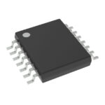 SN74HCS30QPWRQ1
SN74HCS30QPWRQ1 is listed in the Inverter Gates range at ChipApex. The manufacturer field lists Texas Instruments. Its product description is IC GATE NAND 1CH…
Read More
SN74HCS30QPWRQ1 is listed in the Inverter Gates range at ChipApex. The manufacturer field lists Texas Instruments. Its product description is IC GATE NAND 1CH…
Read More
Understand RF detector response, dynamic range and calibration. Compare envelope, logarithmic and RMS behavior before choosing a measurement component.
Read More
SN74HCS30QPWRQ1 is listed in the Inverter Gates range at ChipApex. The manufacturer field lists Texas Instruments. Its product description is IC GATE NAND 1CH…
Read More
Learn how a thermostat in a heater works. Check hysteresis, reset mode, thermal placement and contact ratings before selecting a mechanical control.
Read More
Learn how CPLDs implement hardware logic, compare them with FPGAs and MCUs, and check timing, I/O voltage, startup behavior and programming requirements.
Read More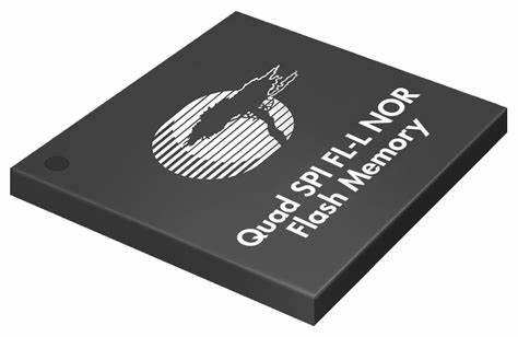
SN74HCS30QPWRQ1 is listed in the Inverter Gates range at ChipApex. The manufacturer field lists Texas Instruments. Its product description is IC GATE NAND 1CH…
Read More
SN74HCS30QPWRQ1 is listed in the Inverter Gates range at ChipApex. The manufacturer field lists Texas Instruments. Its product description is IC GATE NAND 1CH…
Read More
Understand how an electric energy meter measures power and accumulates kWh. Review sensing, phase alignment, calibration and metering IC selection.
Read More
Learn how an analog front end conditions sensor signals. Compare gain, noise, filtering, ADC settling and integration options before selecting components.
Read More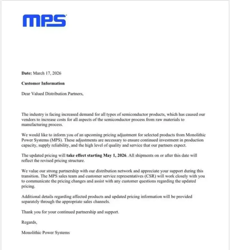
SN74HCS30QPWRQ1 is listed in the Inverter Gates range at ChipApex. The manufacturer field lists Texas Instruments. Its product description is IC GATE NAND 1CH…
Read More
SN74HCS30QPWRQ1 is listed in the Inverter Gates range at ChipApex. The manufacturer field lists Texas Instruments. Its product description is IC GATE NAND 1CH…
Read More
The activity of extra discounts on wholesale prices is in full swing…
Please fill in your contact information and we will send you the latest wholesale price list.





