 ChipApex | Global Electronic Components Supplier

SEARCH
Search Product
Search Post
— IC芯片 | 连接器 | 传感器 | 被动器件 —
Search productSearch post
— IC芯片 | 连接器 | 传感器 | 被动器件 —
Consult the customer manager about the wholesale price.
consultation hotline:86-132-6715-2157
email:[email protected]
Contact the product manager for consultation. One-stop consultation is available.
Do you want a lower wholesale price? Please send us your inquiry and we will reply immediately.
SN74LVC125ANSR is listed in the Buffers, Drivers, Receivers, Transceivers range at ChipApex. The manufacturer field lists Texas Instruments. Its product description is IC BUFFER NON-INVERT 3.6V 14SOP. Review the specifications below when checking this part for your BOM.
The SN74LVC125ANSR is a quadruple bus buffer gate with 3-state outputs manufactured by Texas Instruments. It operates from 1.65V to 3.6V and features independent output-enable inputs for each buffer. The device accepts input voltages up to 5.5V, allowing compatibility with 5V systems while operating at lower supply voltages. It provides a maximum propagation delay of 4.8ns at 3.3V and supports an operating temperature range from -40°C to 125°C. The component is housed in a 14-pin SOP package.
Verify the specific ordering suffix 'NSR' corresponds to the SOP-14 package and tape-and-reel carrier configuration. Confirm that the selected variant meets the required thermal resistance and moisture sensitivity level ratings for the intended manufacturing process. Ensure the component status is active production before finalizing procurement plans.
Select this component when designing mixed-voltage interfaces requiring 3-state buffering between 3.3V logic and 5V peripherals. The independent OE pins allow precise control over bus directionality. Consider the 5.5V input tolerance as a key advantage for direct interfacing without additional level shifters in legacy system designs.
This part belongs to the SN74LVC125A family of quadruple bus buffers. It shares functional characteristics with other LVC series devices but is distinct in its specific pinout and 3-state output configuration. The 'ANSR' designation identifies the specific SOP-14 package and reel packaging format offered by Texas Instruments.
SN74LVC125ADBR
To ensure the high-impedance state during power up or power down, the OE input should be tied to VCC through a pull-up resistor.
The inputs can be driven from either 3.3V or 5V devices, accepting voltages up to 5.5V regardless of the VCC supply level.
Explore related parts through Logic, Integrated Circuits (ICs), all product categories, ChipApex homepage.
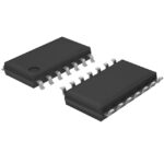 SN74LVC125ANSR
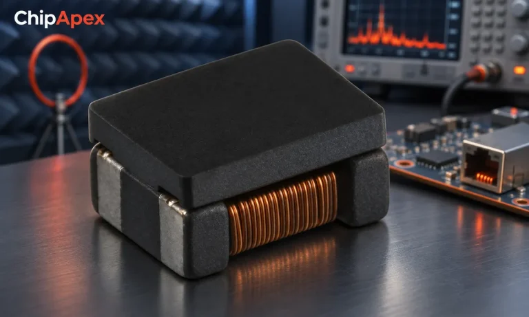
Select a common mode choke using noise frequency, current, insulation and signal integrity. Understand impedance curves, layout and filter limitations.
Read More
SN74LVC125ANSR is listed in the Buffers, Drivers, Receivers, Transceivers range at ChipApex. The manufacturer field lists Texas Instruments. Its product description is IC BUFFER…
Read More
SN74LVC125ANSR is listed in the Buffers, Drivers, Receivers, Transceivers range at ChipApex. The manufacturer field lists Texas Instruments. Its product description is IC BUFFER…
Read More
SN74LVC125ANSR is listed in the Buffers, Drivers, Receivers, Transceivers range at ChipApex. The manufacturer field lists Texas Instruments. Its product description is IC BUFFER…
Read More
SN74LVC125ANSR is listed in the Buffers, Drivers, Receivers, Transceivers range at ChipApex. The manufacturer field lists Texas Instruments. Its product description is IC BUFFER…
Read More
SN74LVC125ANSR is listed in the Buffers, Drivers, Receivers, Transceivers range at ChipApex. The manufacturer field lists Texas Instruments. Its product description is IC BUFFER…
Read More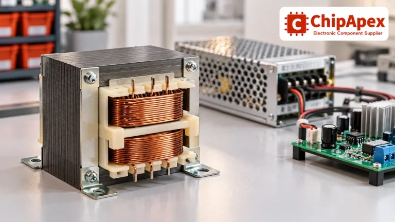
Select power transformers by input frequency, secondary VA, rectifier load, isolation, regulation and inrush. Build a clearer specification for your next RFQ.
Read More
SN74LVC125ANSR is listed in the Buffers, Drivers, Receivers, Transceivers range at ChipApex. The manufacturer field lists Texas Instruments. Its product description is IC BUFFER…
Read More
SN74LVC125ANSR is listed in the Buffers, Drivers, Receivers, Transceivers range at ChipApex. The manufacturer field lists Texas Instruments. Its product description is IC BUFFER…
Read More
SN74LVC125ANSR is listed in the Buffers, Drivers, Receivers, Transceivers range at ChipApex. The manufacturer field lists Texas Instruments. Its product description is IC BUFFER…
Read More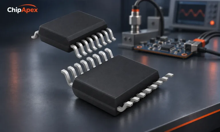
Choose an ADC converter by resolution, sample rate, noise and input design. Review practical tradeoffs and prepare component requirements for ChipApex.
Read More
SN74LVC125ANSR is listed in the Buffers, Drivers, Receivers, Transceivers range at ChipApex. The manufacturer field lists Texas Instruments. Its product description is IC BUFFER…
Read More
The activity of extra discounts on wholesale prices is in full swing…
Please fill in your contact information and we will send you the latest wholesale price list.





