 ChipApex | Global Electronic Components Supplier

SEARCH
Search Product
Search Post
— IC芯片 | 连接器 | 传感器 | 被动器件 —
Search productSearch post
— IC芯片 | 连接器 | 传感器 | 被动器件 —
Consult the customer manager about the wholesale price.
consultation hotline:86-132-6715-2157
email:[email protected]
Contact the product manager for consultation. One-stop consultation is available.
Do you want a lower wholesale price? Please send us your inquiry and we will reply immediately.
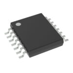
SN74LVC132APWR is listed in the Inverter Gates range at ChipApex. The manufacturer field lists Texas Instruments. Its product description is QUADRUPLE POSITIVE-NAND GATES WI. Review the specifications below when checking this part for your BOM.
The SN74LVC132APWR is a quadruple 2-input NAND gate with Schmitt-trigger inputs in a TSSOP-14 package. It operates from 1.1V to 3.6V and features 5.5V tolerant input pins. The device provides balanced CMOS push-pull outputs capable of sourcing and sinking currents up to 24mA at 3V. Propagation delay ranges from 5.6ns to 15ns depending on voltage and load. It includes ESD protection exceeding 2000V HBM and latch-up performance over 250mA per JESD 17.
Verify the specific ordering suffix 'PW' corresponds to the TSSOP-14 package configuration required for your PCB layout. Confirm that the supply voltage range between 1.1V and 3.6V aligns with your system design. Ensure input signals do not exceed the absolute maximum ratings to prevent permanent damage. Check the latest datasheet revision for any updates to thermal or electrical characteristics before finalizing the bill of materials.
Select this component when noise immunity is critical due to its Schmitt-trigger architecture, which handles slow input transitions effectively. It is suitable for systems requiring 5.5V tolerant interfaces despite lower core operating voltages. Consider the TSSOP-14 package dimensions if space constraints exist. Evaluate the propagation delay specifications against your timing requirements under specific load capacitance conditions.
This part belongs to the SN74LVC132A family of quadruple 2-input NAND gates. The 'PWR' suffix indicates the TSSOP-14 surface-mount package variant. It is designed for low-voltage CMOS applications requiring robust input handling and standard pinout compatibility with other logic families.
SN74LVC132ADR (SOIC-14) offers identical electrical functionality in a different package format. SN74LVC132ABQAR (WQFN-14) provides the same performance in a smaller footprint. Verify pinout compatibility and thermal management requirements when substituting packages.
The Schmitt-trigger architecture provides hysteresis, making the device extremely tolerant to slow or noisy inputs compared to standard CMOS inputs.
Unused inputs must be terminated to either VCC or ground to prevent undefined operational states; they should never be left floating.
Explore related parts through Logic, Integrated Circuits (ICs), all product categories, ChipApex homepage.
 SN74LVC132APWR

SN74LVC132APWR is listed in the Inverter Gates range at ChipApex. The manufacturer field lists Texas Instruments. Its product description is QUADRUPLE POSITIVE-NAND GATES WI.…
Read More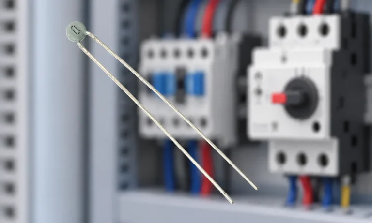
Learn why PTC resistance rises with temperature, how it differs from NTC, and which ratings matter for sensing and protection.
Read More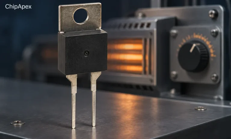
Learn how a thermostat in a heater works. Check hysteresis, reset mode, thermal placement and contact ratings before selecting a mechanical control.
Read More
SN74LVC132APWR is listed in the Inverter Gates range at ChipApex. The manufacturer field lists Texas Instruments. Its product description is QUADRUPLE POSITIVE-NAND GATES WI.…
Read More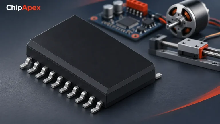
Understand motor controller types, driver functions, startup current, feedback and braking. Use practical checks to match control electronics to your motor.
Read More
SN74LVC132APWR is listed in the Inverter Gates range at ChipApex. The manufacturer field lists Texas Instruments. Its product description is QUADRUPLE POSITIVE-NAND GATES WI.…
Read More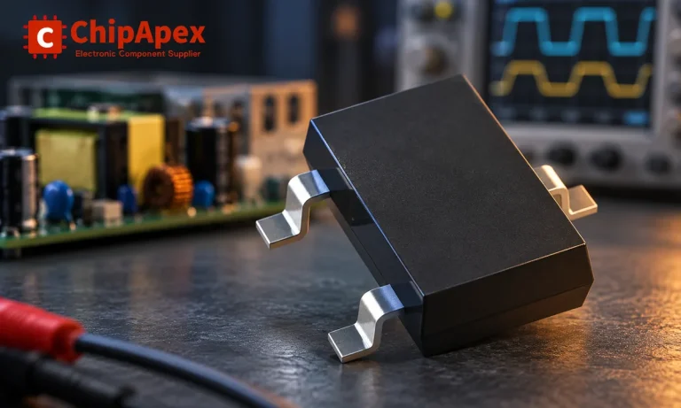
Learn how rectifiers convert AC to DC, compare half-wave and bridge circuits, and select voltage, current, recovery and thermal ratings for your design.
Read More
SN74LVC132APWR is listed in the Inverter Gates range at ChipApex. The manufacturer field lists Texas Instruments. Its product description is QUADRUPLE POSITIVE-NAND GATES WI.…
Read More
SN74LVC132APWR is listed in the Inverter Gates range at ChipApex. The manufacturer field lists Texas Instruments. Its product description is QUADRUPLE POSITIVE-NAND GATES WI.…
Read More
SN74LVC132APWR is listed in the Inverter Gates range at ChipApex. The manufacturer field lists Texas Instruments. Its product description is QUADRUPLE POSITIVE-NAND GATES WI.…
Read More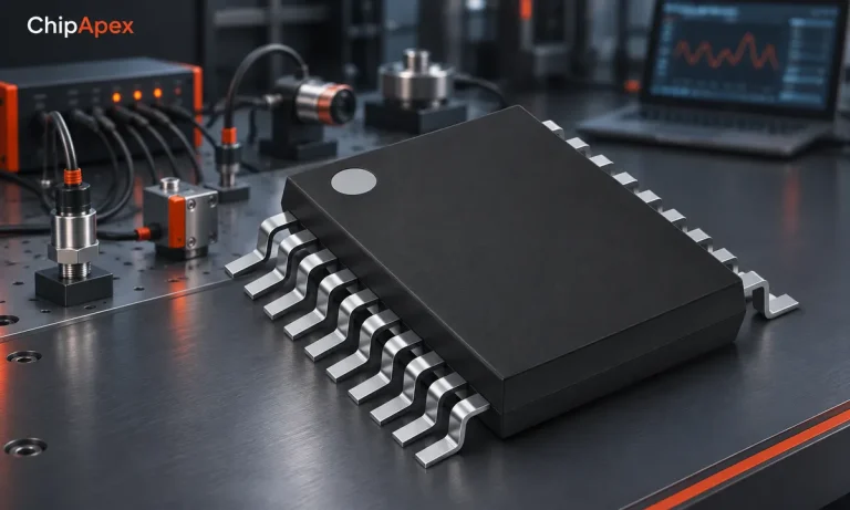
Learn what data acquisition means, from sensors and conditioning to sampling and storage. Review channel timing, wiring, calibration and data quality.
Read More
SN74LVC132APWR is listed in the Inverter Gates range at ChipApex. The manufacturer field lists Texas Instruments. Its product description is QUADRUPLE POSITIVE-NAND GATES WI.…
Read More
The activity of extra discounts on wholesale prices is in full swing…
Please fill in your contact information and we will send you the latest wholesale price list.





