 ChipApex | Global Electronic Components Supplier

SEARCH
Search Product
Search Post
— IC芯片 | 连接器 | 传感器 | 被动器件 —
Search productSearch post
— IC芯片 | 连接器 | 传感器 | 被动器件 —
Consult the customer manager about the wholesale price.
consultation hotline:86-132-6715-2157
email:[email protected]
Contact the product manager for consultation. One-stop consultation is available.
Do you want a lower wholesale price? Please send us your inquiry and we will reply immediately.
SN74LVC16245ADLRG4 is listed in the Buffers, Drivers, Receivers, Transceivers range at ChipApex. The manufacturer field lists Texas Instruments. Its product description is IC TXRX NON-INVERT 3.6V 48SSOP. Review the specifications below when checking this part for your BOM.
The SN74LVC16245ADLRG4 is a 16-bit bus transceiver with 3-state outputs from the Texas Instruments Widebus family. It operates from 1.65 V to 3.6 V and features inputs accepting voltages up to 5.5 V. The maximum propagation delay is 4 ns at 3.3 V, with typical output ground bounce of 2 V at VCC = 3.3 V. It supports mixed-mode signal operation on all asynchronous communication ports. The device includes Ioff circuitry for partial-power-down mode and back-drive protection. ESD protection exceeds JESD 22 standards, rated at 2000 V Human-Body Model and 1000 V Charged-Device Model.
Verify the specific package type matches the design requirements, as the SN74LVC16245A series is available in TSSOP, TVSOP, and SSOP configurations. Confirm that the ordering suffix corresponds to the desired tape and reel quantity and lead finish. Ensure the selected variant meets the required operating temperature range and RoHS compliance status for the target assembly process.
Select this component when interfacing between buses requiring asymmetric voltage translation or mixed-signal environments. The wide supply voltage range accommodates low-power applications down to 1.65 V. Consider the 5.5 V tolerant inputs for direct connection to legacy 5-V logic without additional level shifting components. Evaluate the drive strength and parasitic capacitance against the load requirements to ensure signal integrity.
This device belongs to the Texas Instruments Widebus family, designed for efficient asynchronous data transfer across multiple channels. It functions as either two independent 8-bit transceivers or a single 16-bit transceiver. The architecture minimizes external timing constraints while providing robust isolation capabilities through dedicated output-enable controls.
SN74LVC16245ADGGR
The Ioff circuitry automatically disables the outputs when VCC is 0 V, preventing damaging current backflow through the device into powered buses.
The inputs accept voltages up to 5.5 V regardless of the VCC supply level, enabling safe operation in mixed 3.3-V and 5-V system environments.
Explore related parts through Logic, Integrated Circuits (ICs), all product categories, ChipApex homepage.
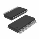 SN74LVC16245ADLRG4

SN74LVC16245ADLRG4 is listed in the Buffers, Drivers, Receivers, Transceivers range at ChipApex. The manufacturer field lists Texas Instruments. Its product description is IC TXRX…
Read MoreSN74LVC16245ADLRG4 is listed in the Buffers, Drivers, Receivers, Transceivers range at ChipApex. The manufacturer field lists Texas Instruments. Its product description is IC TXRX…
Read More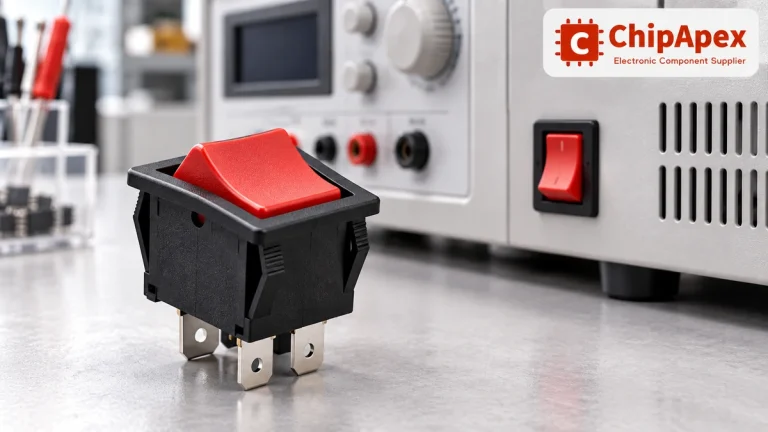
Choose a rocker switch by AC/DC ratings, contact arrangement, illumination, panel fit and sealing. Get practical checks for engineering and component sourcing.
Read More
SN74LVC16245ADLRG4 is listed in the Buffers, Drivers, Receivers, Transceivers range at ChipApex. The manufacturer field lists Texas Instruments. Its product description is IC TXRX…
Read More
SN74LVC16245ADLRG4 is listed in the Buffers, Drivers, Receivers, Transceivers range at ChipApex. The manufacturer field lists Texas Instruments. Its product description is IC TXRX…
Read More
Compare Pt100 and Pt1000 RTDs, two-, three- and four-wire connections, excitation and self-heating. Build an error budget from element to reported temperature.
Read More
SN74LVC16245ADLRG4 is listed in the Buffers, Drivers, Receivers, Transceivers range at ChipApex. The manufacturer field lists Texas Instruments. Its product description is IC TXRX…
Read More
SN74LVC16245ADLRG4 is listed in the Buffers, Drivers, Receivers, Transceivers range at ChipApex. The manufacturer field lists Texas Instruments. Its product description is IC TXRX…
Read More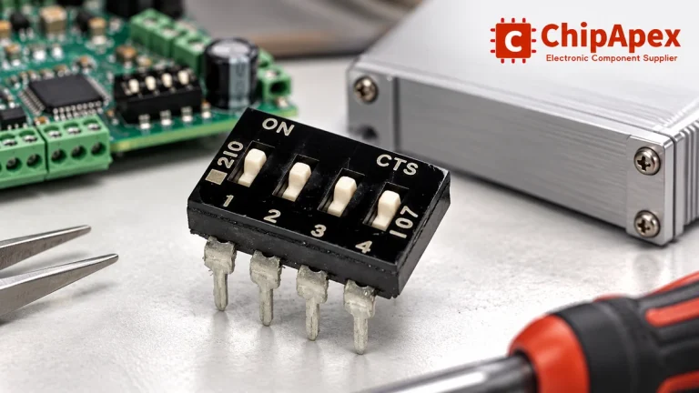
Choose a DIP switch by contact type, coded positions, footprint and signal ratings. Check logic polarity, assembly conditions and PCB configuration behavior.
Read More
Understand UART protocol framing, baud rate and electrical interfaces. Learn 8N1 timing, TX/RX wiring, buffering and practical troubleshooting steps.
Read More
SN74LVC16245ADLRG4 is listed in the Buffers, Drivers, Receivers, Transceivers range at ChipApex. The manufacturer field lists Texas Instruments. Its product description is IC TXRX…
Read More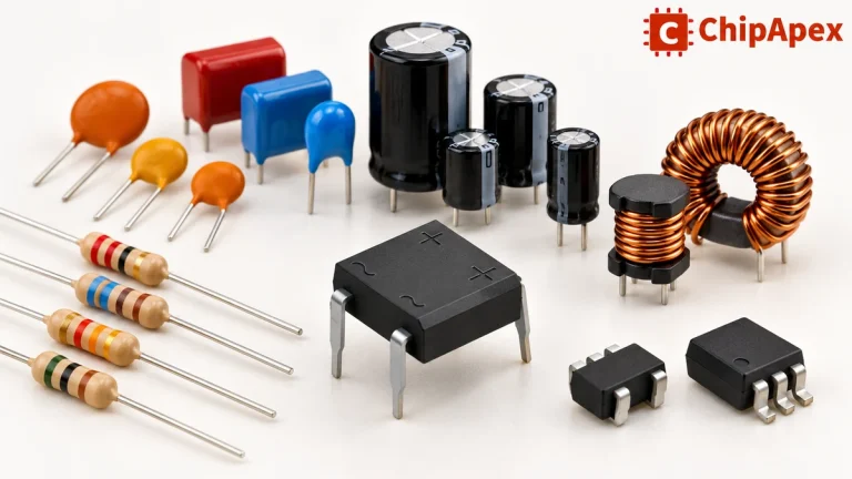
Explore electronic component types, functions, packages and datasheets. Learn selection, replacement and BOM checks before ordering parts for your PCB.
Read More
The activity of extra discounts on wholesale prices is in full swing…
Please fill in your contact information and we will send you the latest wholesale price list.





