 ChipApex | Global Electronic Components Supplier

SEARCH
Search Product
Search Post
— IC芯片 | 连接器 | 传感器 | 被动器件 —
Search productSearch post
— IC芯片 | 连接器 | 传感器 | 被动器件 —
Consult the customer manager about the wholesale price.
consultation hotline:86-132-6715-2157
email:[email protected]
Contact the product manager for consultation. One-stop consultation is available.
Do you want a lower wholesale price? Please send us your inquiry and we will reply immediately.
SNJ54HC164FK is listed in the Shift Registers range at ChipApex. The manufacturer field lists Texas Instruments. Its product description is 8-BIT PARALLEL-OUT SERIAL SHIFT. Review the specifications below when checking this part for your BOM.
The SNJ54HC164FK is an 8-bit parallel-out serial shift register manufactured by Texas Instruments in a 20-pin LCCC package. It operates within a supply voltage range of 2 V to 6 V and supports an operating temperature range from -55°C to 125°C. The device features AND-gated serial inputs (A and B) that control data entry, alongside an asynchronous active-low clear (CLR) input. Clocking occurs on the low-to-high transition of the CLK pin. Electrical characteristics include a maximum ICC of 80 µA at 6 V across the full temperature range, typical propagation delay of 20 ns at 25°C, and output drive capabilities of ±4 mA at 5 V.
Verify the specific ordering suffix FK corresponds to the 20-pin LCCC package configuration. Confirm compliance with MIL-PRF-38535 requirements if military-grade testing is necessary, as standard production processing may not include full parameter testing. Ensure the procurement documentation matches the SNJ prefix indicating JANS or similar qualification levels if applicable to the specific orderable part number.
Select this component when an 8-bit shift register with AND-gated serial inputs is required for harsh environments. The SNJ54HC164FK is suitable for applications demanding extended temperature operation down to -55°C. Consider the 20-pin LCCC package for hermetic sealing needs. Verify that the 2 V to 6 V supply range aligns with system power constraints and that the asynchronous clear functionality meets timing requirements.
This component belongs to the SNx4HC164 family of 8-bit parallel-out serial shift registers. It shares functional specifications with commercial variants like the SN74HC164 but utilizes the SNJ prefix to denote specific packaging and potential qualification standards. The LCCC package variant provides a distinct footprint compared to standard SOIC or PDIP options available within the same logical family.
SN54HC164J
Data enters the shift register only when both serial inputs A and B are high. A low signal on either input inhibits new data entry and resets the first flip-flop to low on the next clock pulse.
The device clocks data on the low-to-high-level transition of the CLK pin. Data can be changed while CLK is high or low, provided minimum setup time requirements are met.
Applying a low signal to the CLR pin asynchronously sets all registers to zero immediately, regardless of the clock state.
Explore related parts through Logic, Integrated Circuits (ICs), all product categories, ChipApex homepage.
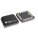 SNJ54HC164FK
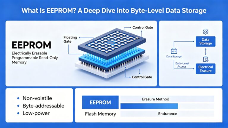
SNJ54HC164FK is listed in the Shift Registers range at ChipApex. The manufacturer field lists Texas Instruments. Its product description is 8-BIT PARALLEL-OUT SERIAL SHIFT.…
Read More
SNJ54HC164FK is listed in the Shift Registers range at ChipApex. The manufacturer field lists Texas Instruments. Its product description is 8-BIT PARALLEL-OUT SERIAL SHIFT.…
Read More
Learn how a JFET works and how to compare bias, leakage, noise and pinout. Review practical selection questions for high-impedance analog circuits.
Read More
SNJ54HC164FK is listed in the Shift Registers range at ChipApex. The manufacturer field lists Texas Instruments. Its product description is 8-BIT PARALLEL-OUT SERIAL SHIFT.…
Read More
Select a DC-DC converter by input range, topology, isolation and temperature. Compare ripple, efficiency and load limits before choosing a component.
Read More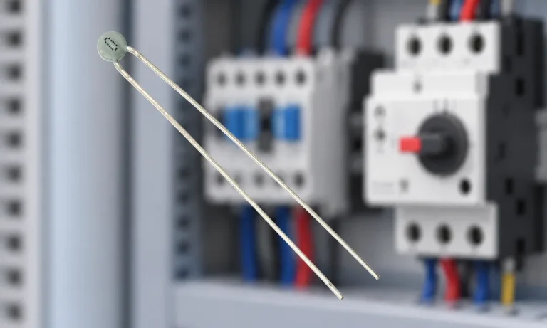
Learn why PTC resistance rises with temperature, how it differs from NTC, and which ratings matter for sensing and protection.
Read More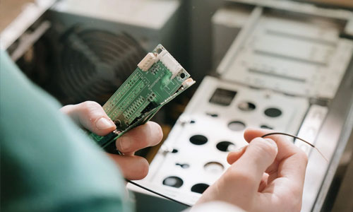
SNJ54HC164FK is listed in the Shift Registers range at ChipApex. The manufacturer field lists Texas Instruments. Its product description is 8-BIT PARALLEL-OUT SERIAL SHIFT.…
Read More
SNJ54HC164FK is listed in the Shift Registers range at ChipApex. The manufacturer field lists Texas Instruments. Its product description is 8-BIT PARALLEL-OUT SERIAL SHIFT.…
Read More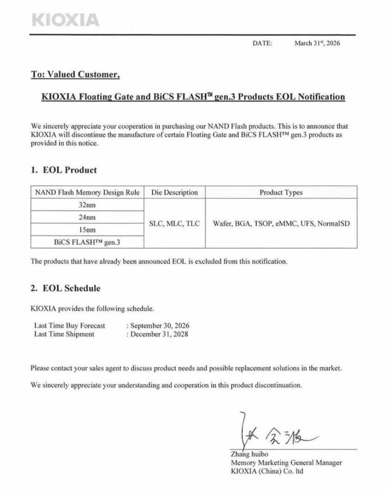
SNJ54HC164FK is listed in the Shift Registers range at ChipApex. The manufacturer field lists Texas Instruments. Its product description is 8-BIT PARALLEL-OUT SERIAL SHIFT.…
Read More
SNJ54HC164FK is listed in the Shift Registers range at ChipApex. The manufacturer field lists Texas Instruments. Its product description is 8-BIT PARALLEL-OUT SERIAL SHIFT.…
Read More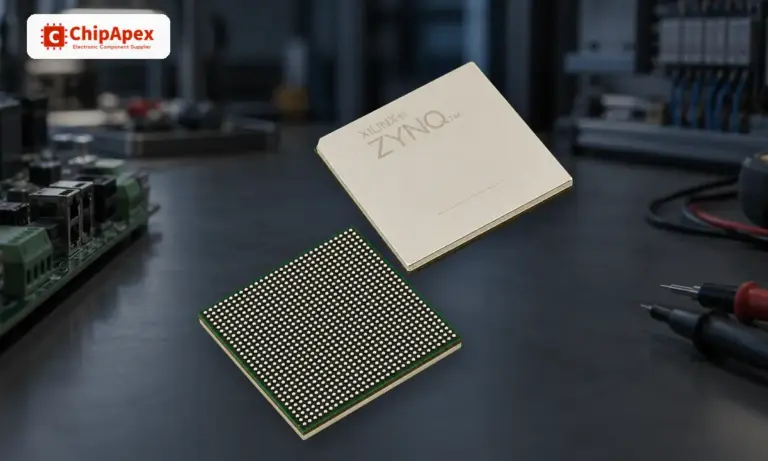
Learn what an integrated circuit is, how ICs work, the main types and the specs to check before choosing a part for your design…
Read More
Learn how a pressure transducer converts pressure into voltage, current, or digital output, and compare pressure references and key selection specs.
Read More
The activity of extra discounts on wholesale prices is in full swing…
Please fill in your contact information and we will send you the latest wholesale price list.





