ChipApex | Global Electronic Components Supplier

SEARCH
Search Product
Search Post
— IC芯片 | 连接器 | 传感器 | 被动器件 —
Search productSearch post
— IC芯片 | 连接器 | 传感器 | 被动器件 —
Consult the customer manager about the wholesale price.
consultation hotline:86-132-6715-2157
email:[email protected]
Contact the product manager for consultation. One-stop consultation is available.
Do you want a lower wholesale price? Please send us your inquiry and we will reply immediately.
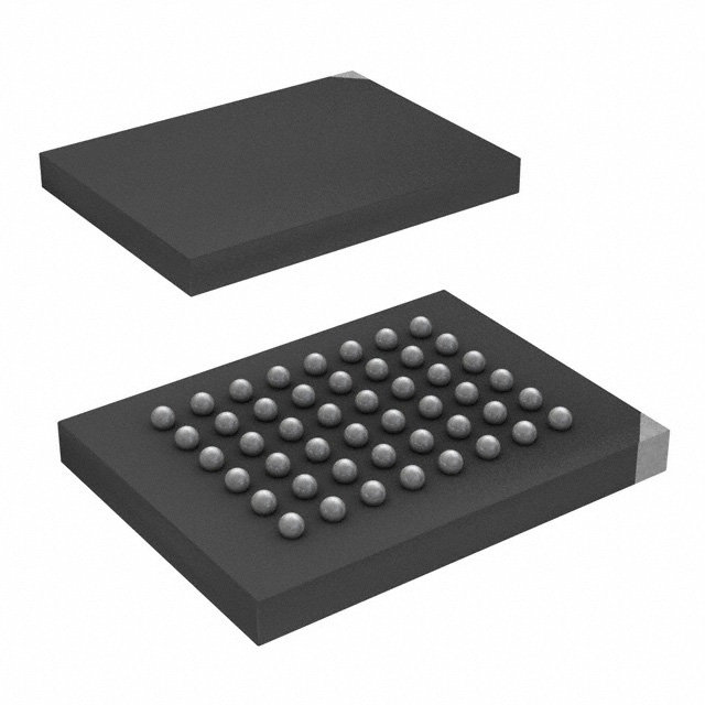
SST39VF400A-70-4C-B3KE is listed in the Memory IC range at ChipApex. The manufacturer field lists Microchip Technology. Its product description is IC FLASH 4MBIT PARALLEL 48TFBGA. Review the specifications below when checking this part for your BOM.
The SST39VF400A-70-4C-B3KE is a 4 Mbit (256K x 16) CMOS Multi-Purpose Flash memory manufactured using SuperFlash technology. It features a parallel asynchronous interface with a typical access time of 70 ns. The device operates on a single voltage supply ranging from 2.7 V to 3.6 V for both read and write operations. It supports sector, block, and chip erase capabilities with uniform sizes. The component is housed in a 48-ball TFBGA package.
Verify the specific suffix 'B3KE' corresponds to the 48-ball TFBGA package and commercial temperature range (0°C to +70°C). Confirm that the '4C' designation aligns with the required operating conditions. Ensure compatibility with the 2.7V to 3.6V single-voltage supply requirement for both read and write cycles.
Select this component when a 4 Mbit capacity with a 16-bit data bus width is required. It is suitable for designs needing a 70 ns access time and a parallel interface. Consider the TFBGA package for surface mount requirements. Verify that the 2.7V minimum operating voltage meets the system's power supply specifications.
This part belongs to the SST39VF series of Multi-Purpose Flash memories. It shares architectural similarities with the SST39LF series but differs in its lower operating voltage range (2.7V vs 3.0V minimum). Both series utilize the same SuperFlash technology and command sets, ensuring functional compatibility within their respective voltage constraints.
SST39VF400A-70-4I-B3KE
The device provides two software means to detect the completion of a write cycle: Data# Polling (DQ7) and Toggle Bit (DQ6).
The memory is organized as 256K words by 16 bits, providing a total capacity of 4 Mbits.
Explore related parts through Memory, Integrated Circuits (ICs), all product categories, ChipApex homepage.
 SST39VF400A-70-4C-B3KE
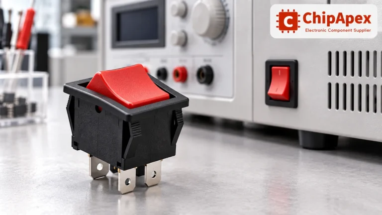
Choose a rocker switch by AC/DC ratings, contact arrangement, illumination, panel fit and sealing. Get practical checks for engineering and component sourcing.
Read More
SST39VF400A-70-4C-B3KE is listed in the Memory IC range at ChipApex. The manufacturer field lists Microchip Technology. Its product description is IC FLASH 4MBIT PARALLEL…
Read More
SST39VF400A-70-4C-B3KE is listed in the Memory IC range at ChipApex. The manufacturer field lists Microchip Technology. Its product description is IC FLASH 4MBIT PARALLEL…
Read More
SST39VF400A-70-4C-B3KE is listed in the Memory IC range at ChipApex. The manufacturer field lists Microchip Technology. Its product description is IC FLASH 4MBIT PARALLEL…
Read More
SST39VF400A-70-4C-B3KE is listed in the Memory IC range at ChipApex. The manufacturer field lists Microchip Technology. Its product description is IC FLASH 4MBIT PARALLEL…
Read More
SST39VF400A-70-4C-B3KE is listed in the Memory IC range at ChipApex. The manufacturer field lists Microchip Technology. Its product description is IC FLASH 4MBIT PARALLEL…
Read More
SST39VF400A-70-4C-B3KE is listed in the Memory IC range at ChipApex. The manufacturer field lists Microchip Technology. Its product description is IC FLASH 4MBIT PARALLEL…
Read More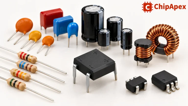
Explore electronic component types, functions, packages and datasheets. Learn selection, replacement and BOM checks before ordering parts for your PCB.
Read More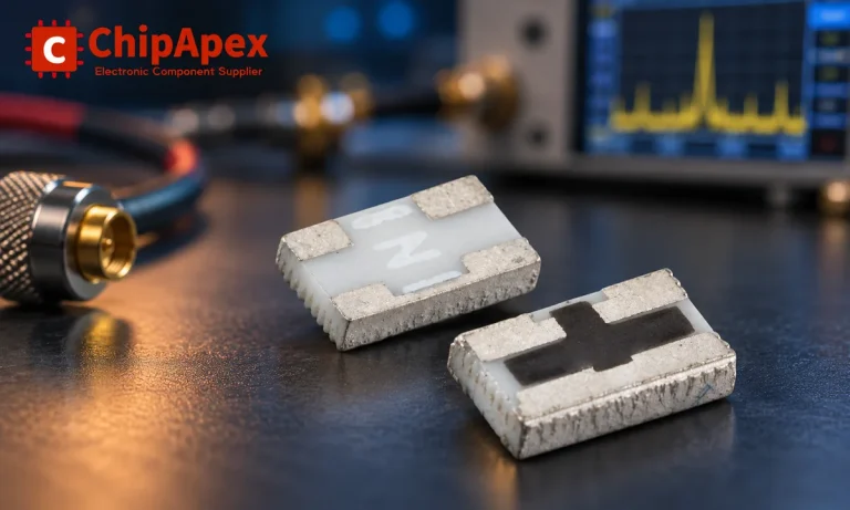
Understand RF attenuator dB values, fixed and programmable types, impedance, power limits and noise tradeoffs before choosing parts for an RF signal path.
Read More
See how a MEMS gyroscope measures angular rate, why its angle estimate drifts, and which range, noise, interface and temperature specs to compare.
Read More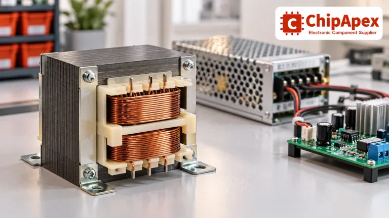
Select power transformers by input frequency, secondary VA, rectifier load, isolation, regulation and inrush. Build a clearer specification for your next RFQ.
Read More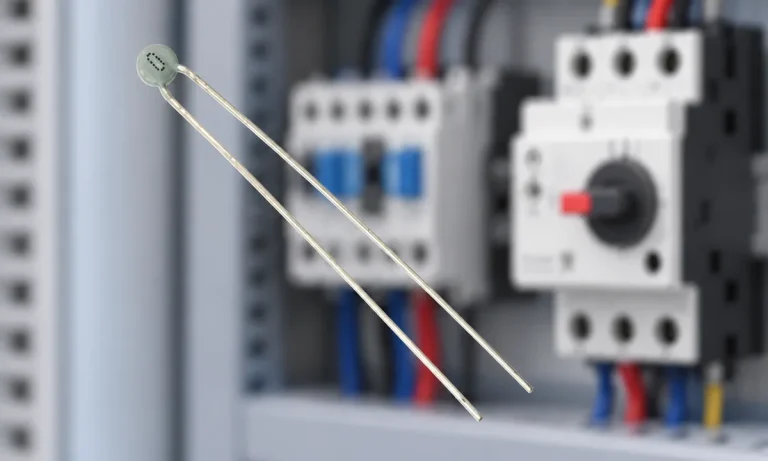
Learn why PTC resistance rises with temperature, how it differs from NTC, and which ratings matter for sensing and protection.
Read More
The activity of extra discounts on wholesale prices is in full swing…
Please fill in your contact information and we will send you the latest wholesale price list.