 ChipApex | Global Electronic Components Supplier

SEARCH
Search Product
Search Post
— IC芯片 | 连接器 | 传感器 | 被动器件 —
Search productSearch post
— IC芯片 | 连接器 | 传感器 | 被动器件 —
Consult the customer manager about the wholesale price.
consultation hotline:86-132-6715-2157
email:[email protected]
Contact the product manager for consultation. One-stop consultation is available.
Do you want a lower wholesale price? Please send us your inquiry and we will reply immediately.
W29N04GVSIAA TR is listed in the Memory IC range at ChipApex. The manufacturer field lists Winbond Electronics. Its product description is IC FLASH 4GBIT ONFI 48TSOP. Review the specifications below when checking this part for your BOM.
The W29N04GVSIAA TR is a 4 Gbit Single-Level Cell (SLC) NAND flash memory from Winbond, organized as 512M x 8 bits. It operates on a single 2.7V to 3.6V power supply with active current consumption of 25mA at 3V and standby current of 10uA. The device supports a multiplexed 8-bit bus interface for data, addresses, and commands. Key performance metrics include a maximum random read time of 25μs, sequential read cycle of 25ns, page program time of 250μs, and block erase time of 2ms. It offers an endurance of 100,000 erase/program cycles and 10-year data retention. The component is housed in a 48-pin TSOP package and functions within an industrial temperature range of -40°C to 85°C.
Verify the specific ordering suffix 'TR' indicates tape and reel packaging when sourcing this component. Confirm that the 'S' package code corresponds to the required 48-pin TSOP form factor for your design. Ensure compatibility with the ONFI interface standards if integrating with third-party controllers. Check for any recent Product Change Notifications regarding manufacturing location or material composition updates.
Select this part for designs requiring high endurance and reliable SLC performance in embedded systems with limited pin counts. The 8-bit parallel interface simplifies controller requirements compared to serial alternatives. Consider the 48-pin TSOP footprint constraints during PCB layout. Verify that the system power supply remains stable within the 2.7V to 3.6V operating range to ensure correct device functionality.
This component belongs to the W29N04GV series of 4 Gbit NAND flash memories. It is designed as a single-chip solution for embedded systems prioritizing low power consumption and compact physical dimensions. The series supports standard NAND interfaces, making it compatible with a wide range of existing memory controllers and host processors used in consumer electronics and industrial equipment.
Direct replacements must match the 4 Gbit density, 8-bit width, and 48-pin TSOP package. Verify that alternative parts support the same 2.7V-3.6V voltage range and industrial temperature specifications. Cross-reference command sets and timing parameters to ensure functional compatibility without firmware modifications.
The memory array is organized into 4,096 erasable blocks, with each block containing 64 programmable pages. Each page consists of 2,048 bytes for main data and 64 bytes for spare data.
The RY/#BY pin is an open-drain output that indicates device status. It outputs low during program, erase, or read operations and returns high when those operations are completed.
Explore related parts through Memory, Integrated Circuits (ICs), all product categories, ChipApex homepage.
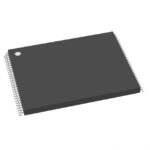 W29N04GVSIAA TR

W29N04GVSIAA TR is listed in the Memory IC range at ChipApex. The manufacturer field lists Winbond Electronics. Its product description is IC FLASH 4GBIT…
Read More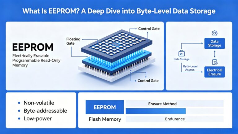
W29N04GVSIAA TR is listed in the Memory IC range at ChipApex. The manufacturer field lists Winbond Electronics. Its product description is IC FLASH 4GBIT…
Read More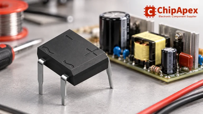
Select a bridge rectifier by reverse voltage, capacitor charging current, startup surge and cooling. Work through a stated DC voltage and ripple example.
Read More
W29N04GVSIAA TR is listed in the Memory IC range at ChipApex. The manufacturer field lists Winbond Electronics. Its product description is IC FLASH 4GBIT…
Read More
W29N04GVSIAA TR is listed in the Memory IC range at ChipApex. The manufacturer field lists Winbond Electronics. Its product description is IC FLASH 4GBIT…
Read More
W29N04GVSIAA TR is listed in the Memory IC range at ChipApex. The manufacturer field lists Winbond Electronics. Its product description is IC FLASH 4GBIT…
Read More
W29N04GVSIAA TR is listed in the Memory IC range at ChipApex. The manufacturer field lists Winbond Electronics. Its product description is IC FLASH 4GBIT…
Read More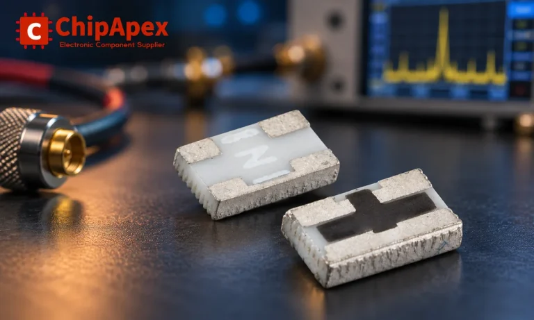
Understand RF attenuator dB values, fixed and programmable types, impedance, power limits and noise tradeoffs before choosing parts for an RF signal path.
Read More
Compare Pt100 and Pt1000 RTDs, two-, three- and four-wire connections, excitation and self-heating. Build an error budget from element to reported temperature.
Read More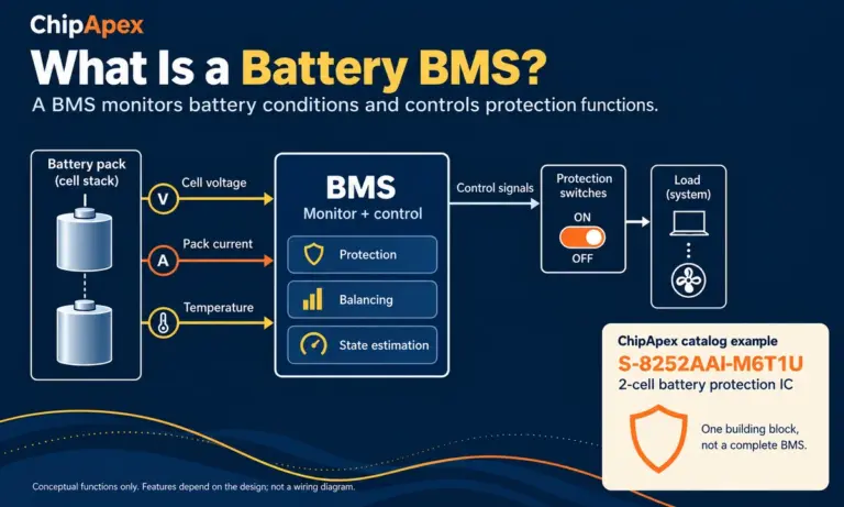
Learn what a battery BMS does, how protection differs from charging, and which pack specifications to check when sourcing BMS components through ChipApex.
Read More
W29N04GVSIAA TR is listed in the Memory IC range at ChipApex. The manufacturer field lists Winbond Electronics. Its product description is IC FLASH 4GBIT…
Read More
W29N04GVSIAA TR is listed in the Memory IC range at ChipApex. The manufacturer field lists Winbond Electronics. Its product description is IC FLASH 4GBIT…
Read More
The activity of extra discounts on wholesale prices is in full swing…
Please fill in your contact information and we will send you the latest wholesale price list.





