ChipApex | Global Electronic Components Supplier
5SGXMA4K2F40I3N
Search Product
Search Post
— IC芯片 | 连接器 | 传感器 | 被动器件 —
Search productSearch post
— IC芯片 | 连接器 | 传感器 | 被动器件 —
Consult the customer manager about the wholesale price.
consultation hotline:86-132-6715-2157
email:[email protected]
Contact the product manager for consultation. One-stop consultation is available.
Do you want a lower wholesale price? Please send us your inquiry and we will reply immediately.
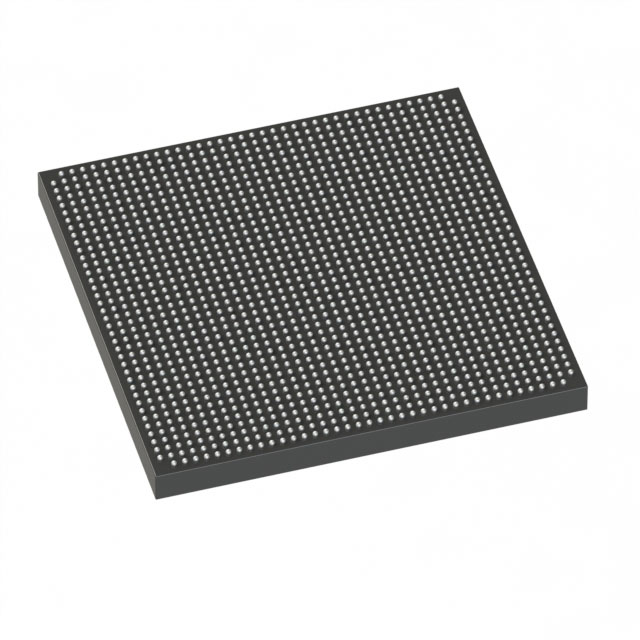
The Altera 5SGXMA4K2F40I3N is a Stratix V GX Field Programmable Gate Array (FPGA) designed for high-performance digital signal processing and networking applications. It features 1900 Logic Array Blocks (LABs), 552 I/O pins, and 24 transceivers capable of data rates up to 14.1 Gb/s. The device includes 37 Mbit of embedded memory and operates at a core voltage of 900 mV within an industrial temperature range of -40°C to +85°C. Packaged in a 1152-pin FBGA, it supports surface-mount installation.
Verify component authenticity through authorized channels as this part may be subject to lifecycle restrictions. Confirm package integrity and moisture sensitivity level handling procedures prior to assembly. Cross-reference datasheet specifications against current design requirements to ensure compatibility with existing system constraints and environmental operating conditions.
Evaluate the trade-off between logic capacity and transceiver count when comparing this model to other Stratix V variants. Ensure the 1152-pin FBGA footprint aligns with PCB layout constraints. Verify that the 900 mV core voltage supply design meets the specific power delivery network requirements for stable operation under maximum load conditions.
This component belongs to the Stratix V GX family, which emphasizes high-speed serial connectivity alongside programmable logic. It serves as a mid-range solution within the series, balancing transceiver availability with logic density. The device represents a mature technology node suitable for established high-performance computing and telecommunications standards.
Publicly confirmed direct substitute part numbers are not available in the provided documentation. Consider reviewing the broader Stratix V GX portfolio for alternative pin counts or performance tiers if exact replacement is required.


 5SGXMA4K2F40I3N
The activity of extra discounts on wholesale prices is in full swing…
Please fill in your contact information and we will send you the latest wholesale price list.