 ChipApex | Global Electronic Components Supplier
5SGXMA5N2F45C1NAC
Search Product
Search Post
— IC芯片 | 连接器 | 传感器 | 被动器件 —
Search productSearch post
— IC芯片 | 连接器 | 传感器 | 被动器件 —
Consult the customer manager about the wholesale price.
consultation hotline:86-132-6715-2157
email:[email protected]
Contact the product manager for consultation. One-stop consultation is available.
Do you want a lower wholesale price? Please send us your inquiry and we will reply immediately.
The Altera 5SGXMA5N2F45C1NA is a Stratix V GX Field Programmable Gate Array (FPGA) designed for high-performance digital signal processing and networking applications. This device features 490,000 logic elements and 185,000 Adaptive Logic Modules (ALMs). It integrates 37 Mbits of embedded memory and includes 48 transceivers capable of data rates up to 14.1 Gb/s. The component operates within a junction temperature range of 0°C to 85°C and utilizes a 1152-ball FCBGA package.
This component belongs to the Stratix V GX family, which is optimized for cost-effective, high-volume applications requiring significant I/O counts and moderate logic density. The 'GX' designation indicates the inclusion of high-speed transceivers suitable for serial communication standards.
The integrated transceivers support data rates up to 14.1 Gb/s.
The device contains 18,500 Logic Array Blocks (LABs).


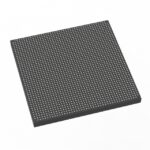 5SGXMA5N2F45C1NAC
The activity of extra discounts on wholesale prices is in full swing…
Please fill in your contact information and we will send you the latest wholesale price list.



