 ChipApex | Global Electronic Components Supplier

SEARCH
Search Product
Search Post
— IC芯片 | 连接器 | 传感器 | 被动器件 —
Search productSearch post
— IC芯片 | 连接器 | 传感器 | 被动器件 —
Consult the customer manager about the wholesale price.
consultation hotline:86-132-6715-2157
email:[email protected]
Contact the product manager for consultation. One-stop consultation is available.
Do you want a lower wholesale price? Please send us your inquiry and we will reply immediately.
5SGXMA7H3F35C4WN is listed in the Field Programmable Gate Array range at ChipApex. The manufacturer field lists Altera. Its product description is IC FPGA 552 I/O 1152FBGA. Review the specifications below when checking this part for your BOM.
The Altera 5SGXMA7H3F35C4WN is a Stratix V GX Field Programmable Gate Array (FPGA) IC featuring 552 I/Os. It utilizes a 1152-BBGA, FCBGA package with dimensions of 35x35 mm. The device contains 622,000 logic elements and 234,720 Adaptive Logic Modules (ALMs). Embedded memory totals 57.16 Mbits, including 50 Mbits of dedicated RAM. It operates at a supply voltage of 900 mV and supports data rates up to 14.1 Gb/s via 24 transceivers. The operating temperature range is -40°C to +85°C.
Verify component authenticity through authorized Intel or Altera distributors. Confirm RoHS compliance and REACH status prior to integration. Check for moisture sensitivity level (MSL 3) handling requirements during storage and assembly. Ensure compatibility with Quartus Prime software versions for programming and configuration. Validate lead times as availability may vary by region.
Select this model when high logic density and significant embedded memory are required alongside high-speed serial connectivity. Compare against other Stratix V variants based on specific I/O counts and transceiver numbers. Consider power consumption profiles and thermal management needs for the target application environment. Ensure design tools support the specific device family features.
This component belongs to the Stratix V GX series, designed for high-performance applications requiring substantial logic resources and fast serial interfaces. It represents a generation of FPGAs focused on bridging high-end processing capabilities with flexible programmability. The part number indicates specific package, speed grade, and temperature range configurations within the broader product line.
Public confirmed substitute part numbers are not available in the provided documentation. Consult official Intel FPGA migration guides for potential next-generation alternatives or compatible pin-to-pin replacements within the same family.
Explore related parts through Embedded, Integrated Circuits (ICs), all product categories, ChipApex homepage.
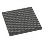 5SGXMA7H3F35C4WN

5SGXMA7H3F35C4WN is listed in the Field Programmable Gate Array range at ChipApex. The manufacturer field lists Altera. Its product description is IC FPGA 552…
Read More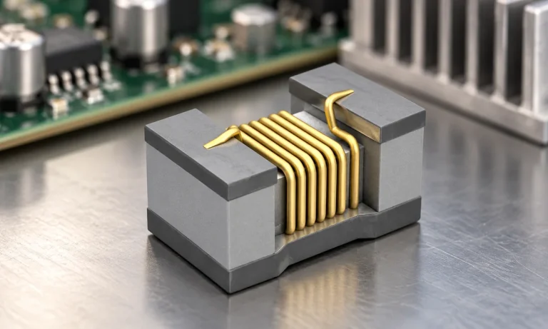
See when an inductor behaves linearly, how DC bias and saturation reduce inductance, and which current and temperature curves to check.
Read More
5SGXMA7H3F35C4WN is listed in the Field Programmable Gate Array range at ChipApex. The manufacturer field lists Altera. Its product description is IC FPGA 552…
Read More
5SGXMA7H3F35C4WN is listed in the Field Programmable Gate Array range at ChipApex. The manufacturer field lists Altera. Its product description is IC FPGA 552…
Read More
5SGXMA7H3F35C4WN is listed in the Field Programmable Gate Array range at ChipApex. The manufacturer field lists Altera. Its product description is IC FPGA 552…
Read More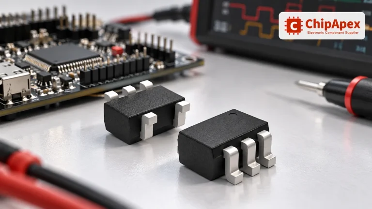
Choose logic inverter ICs by thresholds, supply, output drive and delay. Compare standard and Schmitt-trigger inputs, power sequencing and replacement checks.
Read More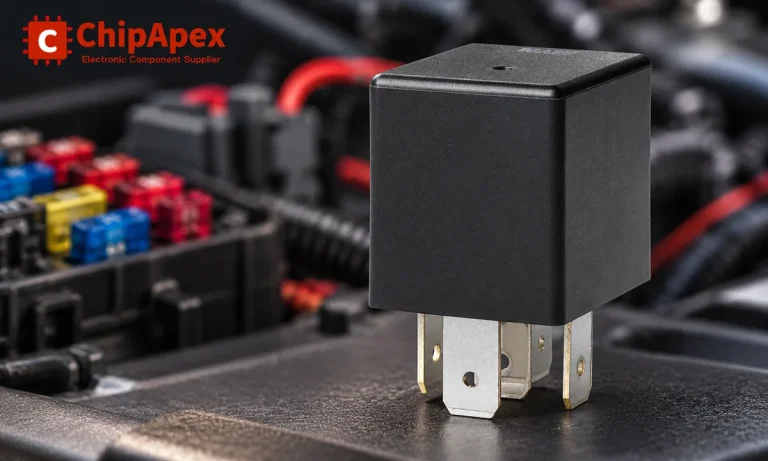
Learn the relay definition, coil and contact operation, NO and NC forms, load ratings and suppression choices. Compare mechanical, reed and solid-state types.
Read More
5SGXMA7H3F35C4WN is listed in the Field Programmable Gate Array range at ChipApex. The manufacturer field lists Altera. Its product description is IC FPGA 552…
Read More
Learn how a pressure transducer converts pressure into voltage, current, or digital output, and compare pressure references and key selection specs.
Read More
5SGXMA7H3F35C4WN is listed in the Field Programmable Gate Array range at ChipApex. The manufacturer field lists Altera. Its product description is IC FPGA 552…
Read More
Choose an AC to DC converter by input range, output demand, isolation, efficiency and thermal derating. Compare architectures and check installation needs.
Read More
5SGXMA7H3F35C4WN is listed in the Field Programmable Gate Array range at ChipApex. The manufacturer field lists Altera. Its product description is IC FPGA 552…
Read More
The activity of extra discounts on wholesale prices is in full swing…
Please fill in your contact information and we will send you the latest wholesale price list.






