 ChipApex | Global Electronic Components Supplier

SEARCH
Search Product
Search Post
— IC芯片 | 连接器 | 传感器 | 被动器件 —
Search productSearch post
— IC芯片 | 连接器 | 传感器 | 被动器件 —
Consult the customer manager about the wholesale price.
consultation hotline:86-132-6715-2157
email:[email protected]
Contact the product manager for consultation. One-stop consultation is available.
Do you want a lower wholesale price? Please send us your inquiry and we will reply immediately.
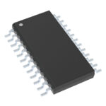
74ACT843SC is listed in the Latches range at ChipApex. The manufacturer field lists onsemi. Its product description is IC D-TYPE TRANSP SGL 9:9 24SOP. Review the specifications below when checking this part for your BOM.
The onsemi 74ACT843SC is a 9-bit transparent latch featuring TTL-compatible inputs and 3-STATE outputs. It operates within a supply voltage range of 4.5V to 5.5V and supports an operating temperature range from -40°C to +85°C. The device utilizes a 24-Lead Small Outline Integrated Circuit (SOIC) package, designated as M24B. Key electrical characteristics include a maximum propagation delay of 10.0 ns at 5.0V with 50 pF load, ensuring high-speed data handling. Quiescent supply current is limited to 80.0 µA, while output drive capability reaches ±24 mA.
Verify the specific ordering suffix against the manufacturer's documentation to confirm packaging type. The standard SC designation indicates SOIC packaging, while appending 'X' denotes Tape and Reel availability. Confirm RoHS compliance status through official material composition documents prior to integration into final assemblies.
Select this component when designing circuits requiring wide data path buffering with transparent latch functionality. Ensure the design accommodates the specified 4.5V to 5.5V supply voltage range. Verify that the 24-pin SOIC footprint aligns with the PCB layout constraints and thermal requirements for the target operating environment.
This component belongs to the ACT logic family, characterized by CMOS technology compatible with TTL input levels. It serves as a bus interface latch designed to replace multiple discrete packages, simplifying board layouts for wider data buses. The device integrates control signals for precise data latching and tri-state bus management.
Check for equivalent 9-bit transparent latches from other manufacturers offering identical pinouts and electrical specifications. Verify compatibility with existing system timing constraints and voltage levels before substitution.
When the Latch Enable (LE) pin is HIGH, the flip-flops appear transparent, allowing the output transition to follow the data input transition immediately.
Data appears on the bus when the Output Enable (OE) pin is LOW. When OE is HIGH, the bus output enters a high impedance state.
The Preset signal overrides the Clear signal. If PRE is LOW, the outputs go HIGH (assuming OE is LOW), regardless of the Clear pin state.
Explore related parts through Logic, Integrated Circuits (ICs), all product categories, ChipApex homepage.
 74ACT843SC

Choose a DIP switch by contact type, coded positions, footprint and signal ratings. Check logic polarity, assembly conditions and PCB configuration behavior.
Read More
74ACT843SC is listed in the Latches range at ChipApex. The manufacturer field lists onsemi. Its product description is IC D-TYPE TRANSP SGL 9:9 24SOP.…
Read More
74ACT843SC is listed in the Latches range at ChipApex. The manufacturer field lists onsemi. Its product description is IC D-TYPE TRANSP SGL 9:9 24SOP.…
Read More
74ACT843SC is listed in the Latches range at ChipApex. The manufacturer field lists onsemi. Its product description is IC D-TYPE TRANSP SGL 9:9 24SOP.…
Read More
74ACT843SC is listed in the Latches range at ChipApex. The manufacturer field lists onsemi. Its product description is IC D-TYPE TRANSP SGL 9:9 24SOP.…
Read More
74ACT843SC is listed in the Latches range at ChipApex. The manufacturer field lists onsemi. Its product description is IC D-TYPE TRANSP SGL 9:9 24SOP.…
Read More74ACT843SC is listed in the Latches range at ChipApex. The manufacturer field lists onsemi. Its product description is IC D-TYPE TRANSP SGL 9:9 24SOP.…
Read More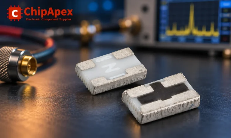
Understand RF attenuator dB values, fixed and programmable types, impedance, power limits and noise tradeoffs before choosing parts for an RF signal path.
Read More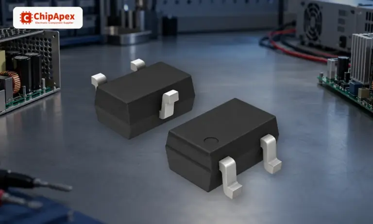
Learn how a diode conducts, how to identify anode and cathode, and when to choose rectifier, TVS, Zener or photodiode types for a circuit.
Read More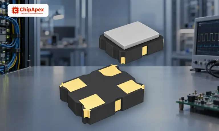
Understand how oscillators generate timing signals, how they differ from crystals, and which frequency, output and stability specs matter when choosing one.
Read More
Learn what an IMU measures, how accelerometers and gyroscopes work together, why orientation estimates drift, and what to compare.
Read More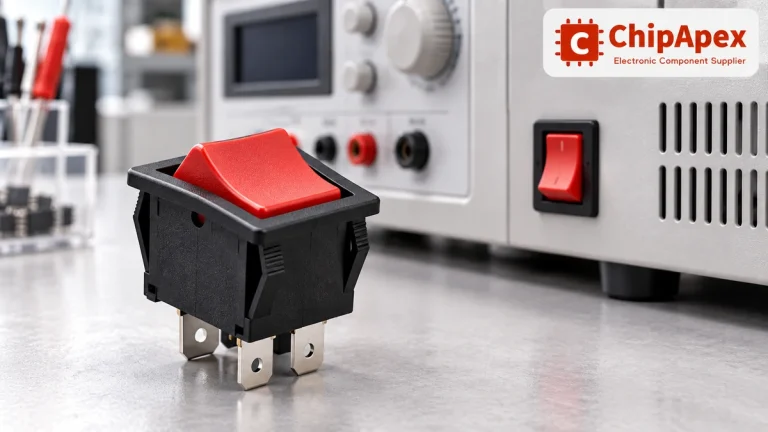
Choose a rocker switch by AC/DC ratings, contact arrangement, illumination, panel fit and sealing. Get practical checks for engineering and component sourcing.
Read More
The activity of extra discounts on wholesale prices is in full swing…
Please fill in your contact information and we will send you the latest wholesale price list.






