 ChipApex | Global Electronic Components Supplier
74AUC1G125DCKRE4
Search Product
Search Post
— IC芯片 | 连接器 | 传感器 | 被动器件 —
Search productSearch post
— IC芯片 | 连接器 | 传感器 | 被动器件 —
Consult the customer manager about the wholesale price.
consultation hotline:86-132-6715-2157
email:[email protected]
Contact the product manager for consultation. One-stop consultation is available.
Do you want a lower wholesale price? Please send us your inquiry and we will reply immediately.
The SN74AUC1G125 is a single bus buffer gate with a 3-state output, part of the AUC logic family optimized for high-speed operation. It operates within a wide voltage range of 0.8 V to 2.7 V and features over-voltage tolerant I/Os supporting up to 3.6 V independent of VCC. The device provides ±8-mA output drive at 1.8 V and achieves a maximum propagation delay of 2.5 ns at 1.8 V with a 30 pF load. It includes an Ioff feature for partial power-down mode and back-drive protection, ensuring low power consumption with a maximum ICC of 10 µA.
Verify the specific package suffix (DCK, DBV, or YZP) matches the required footprint, as the base number covers multiple options. Confirm the 'RE4' suffix indicates the standard tape-and-reel packaging format. Ensure the operating temperature range aligns with system requirements, as this variant supports -40°C to +85°C. Cross-reference the manufacturer's latest orderable addendum for current production status and material compliance details before finalizing procurement.
Select this component when designing systems requiring high-speed buffering between 0.8 V and 2.7 V domains. It is suitable for applications needing over-voltage tolerant inputs without external level shifting. Consider the specific package size constraints, as the DCK, DBV, and YZP options offer different physical footprints. Ensure input transition rates meet the recommended specifications to avoid excessive power consumption or oscillation during operation.
This device belongs to Texas Instruments' AUC (Advanced Ultra-Low Voltage CMOS) logic family, which is engineered for speed and low power. Unlike standard LVC devices, the AUC series is specifically optimized for operation between 1.65 V and 1.95 V, though it functions across a wider 0.8 V to 2.7 V range. The family utilizes unique output structures to maintain signal integrity on short transmission lines without external termination resistors.
SN74AUC1G125DBVR
The Ioff circuitry disables all outputs when the supply pin is held at 0 V. This prevents damaging current backflow through the device when it is powered down, regardless of the input voltages applied.
The ULTTL outputs are balanced drivers designed to maximize transition rates while limiting ringing and transmission line reflections. They are optimized for direct connection to 50- to 65-Ω controlled impedance transmission lines of moderate length.
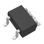 74AUC1G125DCKRE4
The activity of extra discounts on wholesale prices is in full swing…
Please fill in your contact information and we will send you the latest wholesale price list.





