 ChipApex | Global Electronic Components Supplier
74AUP1G132GW-Q100H
Search Product
Search Post
— IC芯片 | 连接器 | 传感器 | 被动器件 —
Search productSearch post
— IC芯片 | 连接器 | 传感器 | 被动器件 —
Consult the customer manager about the wholesale price.
consultation hotline:86-132-6715-2157
email:[email protected]
Contact the product manager for consultation. One-stop consultation is available.
Do you want a lower wholesale price? Please send us your inquiry and we will reply immediately.
The Nexperia 74AUP1G132GW-Q100H is a single 2-input NAND gate with Schmitt-trigger inputs, designed for automotive applications. It operates within a supply voltage range of 0.8 V to 3.6 V and supports an ambient temperature range from -40 °C to +125 °C. The device features low static power consumption (ICC max 0.9 μA at -40°C to +85°C) and IOFF circuitry for partial power-down mode operation. Propagation delay ranges from 1.4 ns to 7.2 ns depending on load capacitance and voltage. It complies with AEC-Q100 Grade 1 standards.
Verify the specific suffix GW corresponds to the TSSOP5 package (SOT353-1) and the Q100 designation confirms AEC-Q100 Grade 1 automotive qualification. Confirm the operating temperature range matches the required -40 °C to +125 °C specification for your application environment before finalizing procurement.
Select this component when a single 2-input NAND function with hysteresis is required in space-constrained designs. The TSSOP5 package offers a compact footprint suitable for high-density PCB layouts. Ensure the design accounts for the specified propagation delays and output drive capabilities across the full 0.8 V to 3.6 V supply range.
This part belongs to the 74AUP1G132-Q100 series of low-power CMOS logic gates. It is manufactured by Nexperia USA Inc. and utilizes the SOT353-1 (TSSOP5) plastic thin shrink small outline package. The marking code for this device is 'aE'.
The datasheet lists the 74AUP1G132GZ-Q100 as an alternative package option (XSON5/SOT8065-1). No other direct functional substitutes are explicitly confirmed in the provided documentation.
Yes, it includes IOFF circuitry that disables the output to prevent damaging backflow current when the device is powered down.
The recommended operating conditions specify a maximum supply voltage (VCC) of 3.6 V.
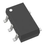 74AUP1G132GW-Q100H
The activity of extra discounts on wholesale prices is in full swing…
Please fill in your contact information and we will send you the latest wholesale price list.





