 ChipApex | Global Electronic Components Supplier

SEARCH
Search Product
Search Post
— IC芯片 | 连接器 | 传感器 | 被动器件 —
Search productSearch post
— IC芯片 | 连接器 | 传感器 | 被动器件 —
Consult the customer manager about the wholesale price.
consultation hotline:86-132-6715-2157
email:[email protected]
Contact the product manager for consultation. One-stop consultation is available.
Do you want a lower wholesale price? Please send us your inquiry and we will reply immediately.
74LV165D,118 is listed in the Shift Registers range at ChipApex. The manufacturer field lists Nexperia USA Inc.. Its product description is IC 8BIT SHIFT REGISTER 16SOIC. Review the specifications below when checking this part for your BOM.
The Nexperia 74LV165D,118 is an 8-bit parallel-in/serial-out shift register housed in a SO16 (SOT109-1) plastic small outline package. It operates within a supply voltage range of 1.0 V to 5.5 V and supports an ambient temperature range from -40 °C to +125 °C. The device features eight parallel data inputs (D0 to D7), a serial data input (DS), and complementary serial outputs (Q7 and Q7). Key control signals include an active LOW parallel load input (PL), a clock enable input (CE), and a LOW-to-HIGH edge-triggered clock input (CP).
Verify that the ordering suffix ',118' corresponds specifically to the SO16 (SOT109-1) package variant. Confirm the component meets the required operating temperature range of -40 °C to +125 °C for your specific application environment. Ensure design safeguards are implemented as the product is not qualified for automotive use unless explicitly stated otherwise.
Select this component for designs requiring wide supply voltage compatibility from 1.0 V to 5.5 V. It is suitable for low power CMOS applications needing direct interface with TTL levels between 2.7 V and 3.6 V. Consider the SO16 package constraints and verify ESD protection requirements against HBM Class 2 and CDM Class C3 standards.
This part belongs to the 74LV series of logic integrated circuits manufactured by Nexperia. The 74LV family is characterized by low voltage operation and CMOS technology. The 74LV165 specifically functions as an 8-bit shift register, distinct from other logic families like HC or HCT which may have different voltage thresholds and performance characteristics.
The 74LV165PW is a compatible alternative featuring a TSSOP16 package instead of the SO16 form factor. Both variants share identical electrical specifications and functionality but differ in physical dimensions and pin pitch.
Data from the parallel inputs D0 to D7 is loaded asynchronously into the shift register when the parallel load input (PL) is held at a LOW voltage level.
When the CE input is LOW, data shifts on the LOW-to-HIGH transitions of the CP input. A HIGH signal on CE disables the CP input, effectively holding the register state.
Yes, the inputs include clamp diodes, which enables the use of current limiting resistors to interface the inputs to voltages in excess of VCC.
Explore related parts through Logic, Integrated Circuits (ICs), all product categories, ChipApex homepage.
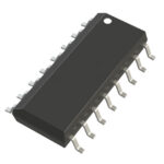 74LV165D,118

Compare RC, crystal and MEMS oscillator circuits. Check ppm, jitter, load capacitance, startup margin and output compatibility before choosing a clock source.
Read More
74LV165D,118 is listed in the Shift Registers range at ChipApex. The manufacturer field lists Nexperia USA Inc.. Its product description is IC 8BIT SHIFT…
Read More
74LV165D,118 is listed in the Shift Registers range at ChipApex. The manufacturer field lists Nexperia USA Inc.. Its product description is IC 8BIT SHIFT…
Read More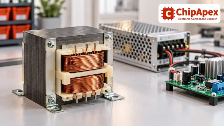
Select power transformers by input frequency, secondary VA, rectifier load, isolation, regulation and inrush. Build a clearer specification for your next RFQ.
Read More
Learn how a diode conducts, how to identify anode and cathode, and when to choose rectifier, TVS, Zener or photodiode types for a circuit.
Read More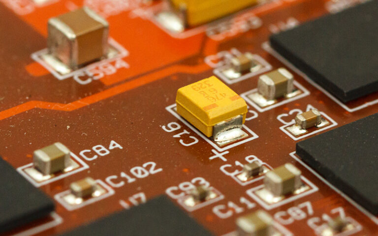
74LV165D,118 is listed in the Shift Registers range at ChipApex. The manufacturer field lists Nexperia USA Inc.. Its product description is IC 8BIT SHIFT…
Read More
74LV165D,118 is listed in the Shift Registers range at ChipApex. The manufacturer field lists Nexperia USA Inc.. Its product description is IC 8BIT SHIFT…
Read More
Select a bridge rectifier by reverse voltage, capacitor charging current, startup surge and cooling. Work through a stated DC voltage and ripple example.
Read More
74LV165D,118 is listed in the Shift Registers range at ChipApex. The manufacturer field lists Nexperia USA Inc.. Its product description is IC 8BIT SHIFT…
Read More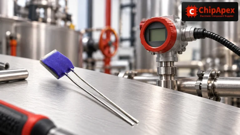
Compare Pt100 and Pt1000 RTDs, two-, three- and four-wire connections, excitation and self-heating. Build an error budget from element to reported temperature.
Read More
74LV165D,118 is listed in the Shift Registers range at ChipApex. The manufacturer field lists Nexperia USA Inc.. Its product description is IC 8BIT SHIFT…
Read More
74LV165D,118 is listed in the Shift Registers range at ChipApex. The manufacturer field lists Nexperia USA Inc.. Its product description is IC 8BIT SHIFT…
Read More
The activity of extra discounts on wholesale prices is in full swing…
Please fill in your contact information and we will send you the latest wholesale price list.






