 ChipApex | Global Electronic Components Supplier
9DBL0255NLGI
Search Product
Search Post
— IC芯片 | 连接器 | 传感器 | 被动器件 —
Search productSearch post
— IC芯片 | 连接器 | 传感器 | 被动器件 —
Consult the customer manager about the wholesale price.
consultation hotline:86-132-6715-2157
email:[email protected]
Contact the product manager for consultation. One-stop consultation is available.
Do you want a lower wholesale price? Please send us your inquiry and we will reply immediately.
The 9DBL0255NLGI is a 3.3V PCIe Gen 1–7 clock multiplexer from Renesas Electronics Corporation. It supports Common Clocked (CC), Separate Reference no Spread (SRnS), and Separate Reference Independent Spread (SRIS) architectures, accommodating PCIe Gen 1 through Gen 7 standards. The device features two differential HCSL inputs and four low-power HCSL (LP-HCSL) outputs with an operating frequency range of 1 MHz to 200 MHz. Key electrical parameters include a typical additive phase jitter of 350 fs RMS and a typical power consumption of 76 mW. It integrates selectable asynchronous or glitch-free switching modes and offers factory-programmable SMBus configurations for user-defined power-up defaults.
Verify the specific suffix 'NLGI' against official Renesas documentation to confirm package type and temperature rating. Ensure compatibility with system voltage requirements and signal integrity specifications before procurement. Cross-reference part numbers with authorized distributors to avoid counterfeit components.
Select this component when designing systems requiring PCIe Gen 1–7 clock distribution with flexible switching modes. Consider the 4mm x 4mm 24-VFQFPN package for space-constrained boards. Evaluate jitter performance against target PHY requirements and verify SMBus programming needs for power-up states.
The 9DBL0255NLGI belongs to Renesas' full-featured PCIe clock family, specifically the 9DML04 series. It serves as a critical timing component in high-speed digital interfaces, providing reliable clock distribution for multi-lane serial links in enterprise and industrial environments.
Check for direct pin-to-pin replacements within the 9DML04 series. Verify that alternative parts support the same PCIe generation standards and switching modes. Confirm package dimensions and thermal characteristics match the existing board layout.
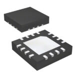 9DBL0255NLGI
The activity of extra discounts on wholesale prices is in full swing…
Please fill in your contact information and we will send you the latest wholesale price list.







