 ChipApex | Global Electronic Components Supplier
9DBL0851CKILF
Search Product
Search Post
— IC芯片 | 连接器 | 传感器 | 被动器件 —
Search productSearch post
— IC芯片 | 连接器 | 传感器 | 被动器件 —
Consult the customer manager about the wholesale price.
consultation hotline:86-132-6715-2157
email:[email protected]
Contact the product manager for consultation. One-stop consultation is available.
Do you want a lower wholesale price? Please send us your inquiry and we will reply immediately.
The 9DBL0851CKILF is a zero-delay buffer (ZDB) clock distribution IC from Renesas Electronics, designed for PCI Express applications. It features one differential input and eight low-power HCSL outputs with an integrated 85Ω termination impedance. The device operates on a single 3.3V supply within a voltage range of 3.135V to 3.465V. It supports input frequencies up to 200MHz and functions in fan-out mode between 1MHz and 200MHz. The component is housed in a 48-VFQFPN package measuring 6mm x 6mm and is rated for operation across a temperature range of -40°C to +85°C.
Verify the specific suffix 'CKILF' against the manufacturer's current datasheet to confirm pinout compatibility and RoHS status. Check for Product Change Notifications regarding assembly sites or material updates. Confirm moisture sensitivity level handling requirements prior to soldering.
Select this model when an 85Ω termination is required for the specific trace impedance of the target design. Ensure the system power supply remains within the 3.135V to 3.465V range. Verify that the 48-VFQFPN package dimensions fit the available PCB real estate compared to other variants in the 9DBL0x series.
This component belongs to the 9DBL0x family of low-power PCIe clock buffers. It shares architectural similarities with the 9DBL0841 and 9DBL0641 models but differs in output count and termination resistance. The 'C' designation typically indicates a specific revision or feature set within the Renesas portfolio.
Publicly confirmed direct substitutes are not listed in the provided documentation. Evaluate the 9DBL0841CKILFT if 100Ω termination is acceptable, though package and electrical differences exist.
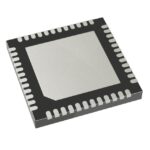 9DBL0851CKILF
The activity of extra discounts on wholesale prices is in full swing…
Please fill in your contact information and we will send you the latest wholesale price list.






