 ChipApex | Global Electronic Components Supplier
9FGL0451DKILFT
Search Product
Search Post
— IC芯片 | 连接器 | 传感器 | 被动器件 —
Search productSearch post
— IC芯片 | 连接器 | 传感器 | 被动器件 —
Consult the customer manager about the wholesale price.
consultation hotline:86-132-6715-2157
email:[email protected]
Contact the product manager for consultation. One-stop consultation is available.
Do you want a lower wholesale price? Please send us your inquiry and we will reply immediately.
The Renesas 9FGL0451DKILFT is a 3.3V PCIe Gen1-5 clock generator providing four differential outputs and one LVCMOS reference output. It operates at 100MHz with a 25MHz input frequency, housed in a 32-VFQFPN package (5x5mm). Key electrical specifications include 90fs RMS typical jitter for PCIe Gen5 Common Clocked mode, less than 50ps cycle-to-cycle jitter, and zero ppm synthesis error. The device supports integrated 85Ω or 100Ω terminations and features SMBus-selectable spread spectrum options.
Verify the specific suffix 'KILFT' against the manufacturer's official documentation to confirm tape-and-reel packaging and RoHS compliance status. Ensure that the required spread spectrum configuration matches the pin-strapped defaults or SMBus programming capabilities defined in the datasheet.
Select this model for designs requiring four differential PCIe clock outputs with integrated termination. Verify compatibility with the target PCIe generation's jitter requirements, specifically noting the 90fs RMS typical performance in CC mode. Confirm that the 32-VFQFPN package dimensions fit the PCB layout constraints.
This component belongs to the 9FGL02x1/04x1/06x1/08x1D family of 3.3V PCIe clock generators. The '04' designation indicates four differential outputs, while the '51' variant typically specifies the -0.5% spread spectrum capability. It serves as a central timing source for high-speed serial interfaces compliant with PCI Express standards.
Direct replacements within the same family include the 9FGL0441D for non-spread spectrum applications. Other variants like the 9FGL02x1D or 9FGL06x1D offer different output counts but share similar architectural features.
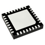 9FGL0451DKILFT
The activity of extra discounts on wholesale prices is in full swing…
Please fill in your contact information and we will send you the latest wholesale price list.





