ChipApex | Global Electronic Components Supplier

SEARCH
Search Product
Search Post
— IC芯片 | 连接器 | 传感器 | 被动器件 —
Search productSearch post
— IC芯片 | 连接器 | 传感器 | 被动器件 —
Consult the customer manager about the wholesale price.
consultation hotline:86-132-6715-2157
email:[email protected]
Contact the product manager for consultation. One-stop consultation is available.
Do you want a lower wholesale price? Please send us your inquiry and we will reply immediately.
AD8099ACP-R2 is listed in the Instrumentation, Op Amps, Buffer Amps range at ChipApex. The manufacturer field lists Analog Devices Inc.. Its product description is IC OPAMP VF ULN ULDIST 8LFCSP. Review the specifications below when checking this part for your BOM.
The AD8099 is an ultralow noise and distortion voltage feedback operational amplifier designed for high-speed signal processing. It features a gain bandwidth product of 3.8 GHz, with −3 dB bandwidths of 700 MHz at G = +2 and 550 MHz at G = +10. The device offers a slew rate of 475 V/µs at G = +2 and 1350 V/µs at G = +10. Input voltage noise is 0.95 nV/√Hz, while harmonic distortion reaches −92 dBc (2nd harmonic) and −105 dBc (3rd harmonic) at 10 MHz with G = +2. It operates on supply voltages from 5 V to 12 V with a quiescent current of 15 mA.
Verify the specific package variant against the datasheet ordering guide, as the AD8099 is available in both SOIC-EP and LFCSP packages with distinct pinouts. Confirm that the required gain configuration matches the external compensation requirements specified for the selected package type. Ensure the operating temperature range aligns with the extended industrial rating of −40°C to +125°C.
Select this component for applications requiring minimal trade-offs between bandwidth and distortion at low gains. The external compensation network allows designers to tailor the closed-loop response for specific gain settings. Consider the package choice carefully, as the SOIC and LFCSP variants exhibit different capacitive load driving capabilities due to output inductance differences.
The AD8099 is part of Analog Devices' portfolio of high-speed voltage feedback amplifiers. It is engineered using the extra fast complimentary bipolar (XFCB) process to achieve performance levels previously associated with fully uncompensated amplifiers. The device is suitable for 16-bit and 18-bit systems where precision and speed are critical.
No direct public substitute part numbers are confirmed in the provided documentation.
Pulling the DISABLE pin low activates a high-impedance state. Pulling it within 0.7 V of the positive supply enables input bias current cancellation, reducing bias current below 200 nA.
External compensation allows the user to set the gain bandwidth product and optimize the closed-loop response for minimal peaking, particularly at gains lower than 15.
Explore related parts through Amplifiers, Linear, Integrated Circuits (ICs), all product categories.
 AD8099ACP-R2
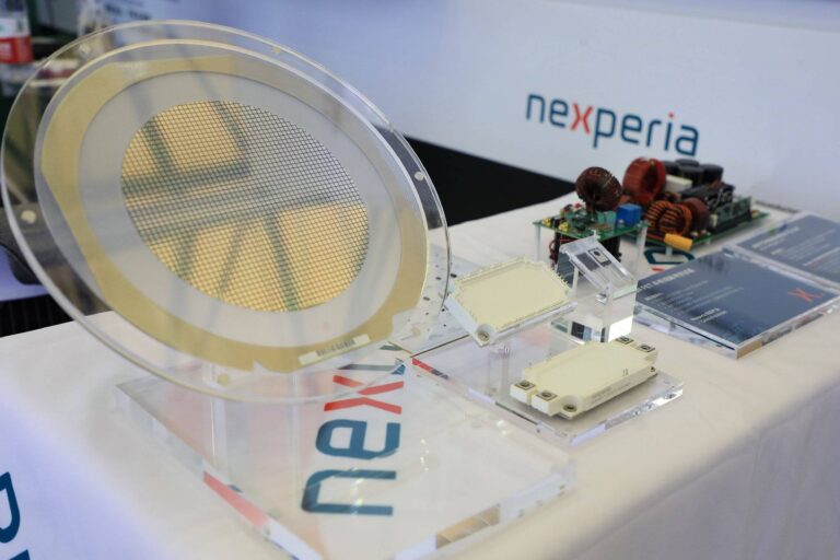
AD8099ACP-R2 is listed in the Instrumentation, Op Amps, Buffer Amps range at ChipApex. The manufacturer field lists Analog Devices Inc.. Its product description is…
Read More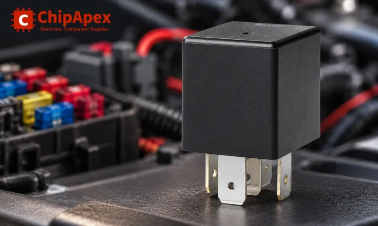
Learn the relay definition, coil and contact operation, NO and NC forms, load ratings and suppression choices. Compare mechanical, reed and solid-state types.
Read More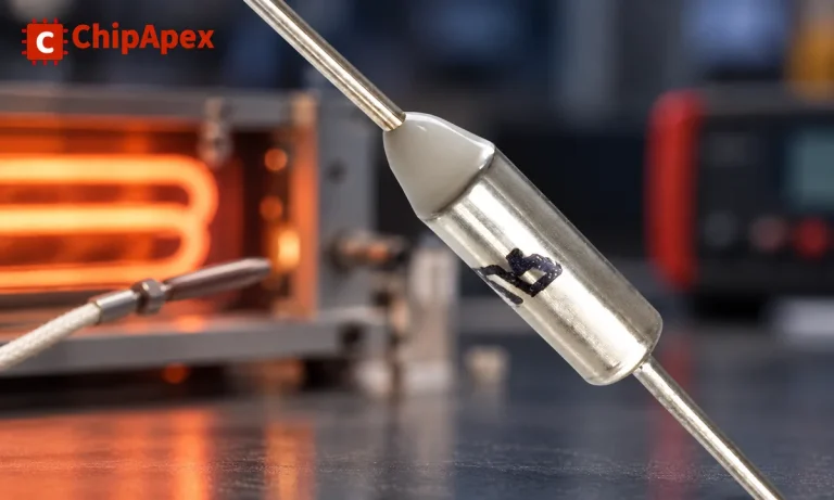
Understand thermal fuse operation, Tf, Th and Tm, electrical ratings and mounting. Check temperature limits and replacement requirements for your design.
Read More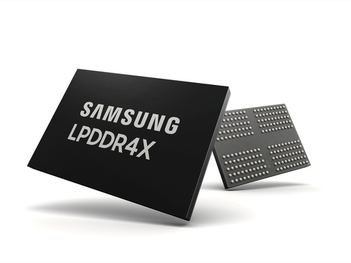
AD8099ACP-R2 is listed in the Instrumentation, Op Amps, Buffer Amps range at ChipApex. The manufacturer field lists Analog Devices Inc.. Its product description is…
Read More
AD8099ACP-R2 is listed in the Instrumentation, Op Amps, Buffer Amps range at ChipApex. The manufacturer field lists Analog Devices Inc.. Its product description is…
Read More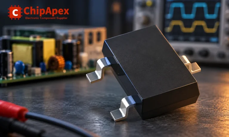
Learn how rectifiers convert AC to DC, compare half-wave and bridge circuits, and select voltage, current, recovery and thermal ratings for your design.
Read More
AD8099ACP-R2 is listed in the Instrumentation, Op Amps, Buffer Amps range at ChipApex. The manufacturer field lists Analog Devices Inc.. Its product description is…
Read More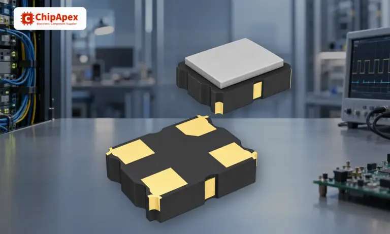
Understand how oscillators generate timing signals, how they differ from crystals, and which frequency, output and stability specs matter when choosing one.
Read More
AD8099ACP-R2 is listed in the Instrumentation, Op Amps, Buffer Amps range at ChipApex. The manufacturer field lists Analog Devices Inc.. Its product description is…
Read More
AD8099ACP-R2 is listed in the Instrumentation, Op Amps, Buffer Amps range at ChipApex. The manufacturer field lists Analog Devices Inc.. Its product description is…
Read More
AD8099ACP-R2 is listed in the Instrumentation, Op Amps, Buffer Amps range at ChipApex. The manufacturer field lists Analog Devices Inc.. Its product description is…
Read More
AD8099ACP-R2 is listed in the Instrumentation, Op Amps, Buffer Amps range at ChipApex. The manufacturer field lists Analog Devices Inc.. Its product description is…
Read More
The activity of extra discounts on wholesale prices is in full swing…
Please fill in your contact information and we will send you the latest wholesale price list.