ChipApex | Global Electronic Components Supplier
AD9102BCPZ
Search Product
Search Post
— IC芯片 | 连接器 | 传感器 | 被动器件 —
Search productSearch post
— IC芯片 | 连接器 | 传感器 | 被动器件 —
Consult the customer manager about the wholesale price.
consultation hotline:86-132-6715-2157
email:[email protected]
Contact the product manager for consultation. One-stop consultation is available.
Do you want a lower wholesale price? Please send us your inquiry and we will reply immediately.
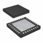
The AD9102BCPZ is a low-power, 14-bit digital-to-analog converter (DAC) and waveform generator from Analog Devices. It integrates on-chip pattern memory for complex waveform generation with a direct digital synthesizer (DDS). The device supports DAC sampling rates of up to 180 MSPS and features differential current outputs with a maximum of 8 mA at 3.3 V. It operates with flexible power supply voltages ranging from 1.8 V to 3.3 V. Key specifications include an SFDR of 87 dBc at a 10 MHz output and a phase noise of −150 dBc/Hz at 1 kHz offset. The component is housed in a small footprint, 32-lead, 5 mm × 5 mm LFCSP package.
Verify the specific ordering suffix against official documentation to ensure correct packaging and temperature grade. Confirm availability through authorized distributors as stock levels fluctuate. Ensure compliance with RoHS standards and check for any recent product change notices that may affect pinout or electrical characteristics prior to final procurement.
Select this component for applications requiring high integration of DDS and pattern memory within a compact form factor. Consider the 1.8 V to 3.3 V operating range for compatibility with various system power rails. Evaluate the 180 MSPS maximum clock rate against the required signal bandwidth. Ensure thermal management strategies account for the 30.18 °C/W junction-to-ambient thermal resistance in the LFCSP package.
The AD9102 belongs to the TxDAC® series of high-performance digital-to-analog converters. It is designed to replace discrete solutions combining DDS, DAC, and memory components. The BC sub-series typically denotes a specific temperature grade and package variant within the broader AD9102 family, optimized for portable and low-power applications.
Public confirmed substitute part numbers are not available in the provided source material.
 AD9102BCPZ
The activity of extra discounts on wholesale prices is in full swing…
Please fill in your contact information and we will send you the latest wholesale price list.