 ChipApex | Global Electronic Components Supplier

SEARCH
Search Product
Search Post
— IC芯片 | 连接器 | 传感器 | 被动器件 —
Search productSearch post
— IC芯片 | 连接器 | 传感器 | 被动器件 —
Consult the customer manager about the wholesale price.
consultation hotline:86-132-6715-2157
email:[email protected]
Contact the product manager for consultation. One-stop consultation is available.
Do you want a lower wholesale price? Please send us your inquiry and we will reply immediately.
ADC09SJ800AAVTQ1 is listed in the Analog To Digital Converters (ADC) range at ChipApex. The manufacturer field lists Texas Instruments. Its product description is IC ANALOG TO DIGITAL CONVERTER. Review the specifications below when checking this part for your BOM.
The ADC09SJ800AAVTQ1 is a single-channel, 9-bit analog-to-digital converter (ADC) operating at an 800 MSPS sampling rate. It features a non-interleaved architecture with a full-power input bandwidth of 6 GHz and supports direct RF sampling up to 4 GHz. The device utilizes a JESD204C serial interface supporting baud rates up to 17.16 Gbps with 64B/66B or 8B/10B encoding. Key performance metrics include a signal-to-noise ratio (SNR) of 53.5 dBFS and an effective number of bits (ENOB) of 8.51 bits at –1dBFS and 97 MHz. Power consumption is 840 mW at maximum speed, powered by 1.1 V and 1.9 V supplies.
Verify the specific ordering suffix against official documentation to confirm package type and temperature grade. Ensure that any additional characters in the part number do not alter the electrical characteristics or functional capabilities defined in the datasheet. Cross-reference the manufacturer's current product status to confirm availability and production lifecycle stage before finalizing procurement plans.
Select this component when a single-channel, high-speed data conversion solution is required for automotive environments. The 6 GHz bandwidth accommodates both FMCW and pulsed LiDAR architectures. Verify that the system can accommodate the 840 mW power dissipation and that the JESD204C lane configuration aligns with the target FPGA or ASIC transceiver capabilities.
This device belongs to the ADC09xJ800-Q1 family, which includes quad (ADC09QJ800-Q1) and dual (ADC09DJ800-Q1) channel variants. All members share identical core specifications, including the 9-bit resolution, 800 MSPS rate, and 6 GHz bandwidth. The primary distinction lies in the number of analog input channels and the corresponding JESD204C lane requirements.
Direct replacements within the same family include the ADC09QJ800-Q1 and ADC09DJ800-Q1. These devices offer identical electrical performance but provide multiple channels instead of a single channel. System designers must account for the additional unused channels and adjust PCB layout and pin connections accordingly.
The JESD204C serialized interface supports a maximum baud rate of 17.16 Gbps.
Yes, the device supports Subclass-1 of the JESD204C standard, which provides deterministic latency for synchronized multi-device systems.
The device features an optional internal sampling clock generation circuit comprising a phase-locked loop (PLL) and a voltage-controlled oscillator (VCO) operating between 7.2 GHz and 8.2 GHz.
Explore related parts through Data Acquisition, Integrated Circuits (ICs), all product categories, ChipApex homepage.
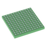 ADC09SJ800AAVTQ1

ADC09SJ800AAVTQ1 is listed in the Analog To Digital Converters (ADC) range at ChipApex. The manufacturer field lists Texas Instruments. Its product description is IC…
Read More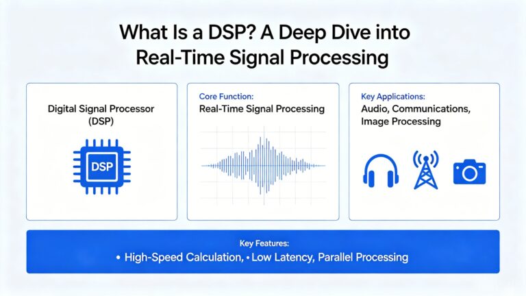
ADC09SJ800AAVTQ1 is listed in the Analog To Digital Converters (ADC) range at ChipApex. The manufacturer field lists Texas Instruments. Its product description is IC…
Read More
Choose an AC to DC converter by input range, output demand, isolation, efficiency and thermal derating. Compare architectures and check installation needs.
Read More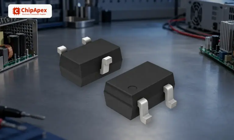
Learn how a diode conducts, how to identify anode and cathode, and when to choose rectifier, TVS, Zener or photodiode types for a circuit.
Read More
ADC09SJ800AAVTQ1 is listed in the Analog To Digital Converters (ADC) range at ChipApex. The manufacturer field lists Texas Instruments. Its product description is IC…
Read More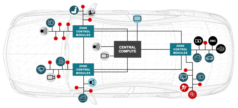
ADC09SJ800AAVTQ1 is listed in the Analog To Digital Converters (ADC) range at ChipApex. The manufacturer field lists Texas Instruments. Its product description is IC…
Read More
Select MOV varistors by continuous voltage, clamping behavior, surge waveform and repetition. Check thermal disconnection, fuse coordination and replacements.
Read More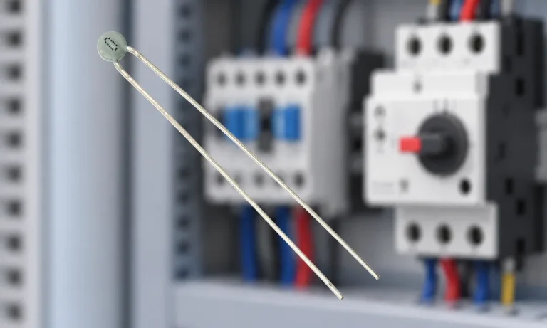
Learn why PTC resistance rises with temperature, how it differs from NTC, and which ratings matter for sensing and protection.
Read More
ADC09SJ800AAVTQ1 is listed in the Analog To Digital Converters (ADC) range at ChipApex. The manufacturer field lists Texas Instruments. Its product description is IC…
Read More
Learn what an IMU measures, how accelerometers and gyroscopes work together, why orientation estimates drift, and what to compare.
Read More
ADC09SJ800AAVTQ1 is listed in the Analog To Digital Converters (ADC) range at ChipApex. The manufacturer field lists Texas Instruments. Its product description is IC…
Read More
ADC09SJ800AAVTQ1 is listed in the Analog To Digital Converters (ADC) range at ChipApex. The manufacturer field lists Texas Instruments. Its product description is IC…
Read More
The activity of extra discounts on wholesale prices is in full swing…
Please fill in your contact information and we will send you the latest wholesale price list.




