 ChipApex | Global Electronic Components Supplier

SEARCH
Search Product
Search Post
— IC芯片 | 连接器 | 传感器 | 被动器件 —
Search productSearch post
— IC芯片 | 连接器 | 传感器 | 被动器件 —
Consult the customer manager about the wholesale price.
consultation hotline:86-132-6715-2157
email:[email protected]
Contact the product manager for consultation. One-stop consultation is available.
Do you want a lower wholesale price? Please send us your inquiry and we will reply immediately.
ADC10D020CIVSX/NOPB is listed in the Analog To Digital Converters (ADC) range at ChipApex. The manufacturer field lists Texas Instruments. Its product description is IC ADC 10BIT TWO-STEP 48TQFP. Review the specifications below when checking this part for your BOM.
The ADC10D020CIVSX/NOPB is a dual-channel, 10-bit CMOS analog-to-digital converter manufactured by Texas Instruments. It supports sampling rates up to 30 MSPS with typical power consumption of 150 mW from a single +3.0V supply. The device features an internal sample-and-hold circuit and reference capability, ensuring no missing codes across the operating temperature range. Key electrical parameters include a typical Effective Number of Bits (ENOB) of 9.5 bits, a Differential Non-Linearity (DNL) of ±0.35 LSB, and a Signal-to-Noise Ratio (SNR) of 59 dB at 1 MHz input frequency. It operates within an industrial temperature range of -40°C to +85°C.
Verify the specific suffix 'CIVSX' against the manufacturer's official documentation to confirm package type and temperature grade details. Ensure compatibility with the required digital output driver supply voltage (VDR) range of +1.5V to VD for system interfacing. Confirm that the 48-pin TQFP package dimensions align with the target PCB layout constraints.
Select this component when a dual-channel, low-power solution is required for mid-speed signal acquisition. The device is suitable for designs needing flexible output formatting via the OS pin. Consider the 2.5 to 3 clock cycle pipeline latency when designing timing-critical digital interfaces. Ensure the external reference voltage (VREF) is maintained between 0.8V and 1.5V for optimal performance.
This part belongs to the ADC10D020 family of high-performance, low-power CMOS A/D converters. The series is designed for applications requiring simultaneous sampling of two channels with minimal power dissipation. The device utilizes a unique two-stage architecture to achieve high linearity and speed while maintaining a simple single-supply operation profile.
Direct replacements should be sought within the ADC10D020 family variants. Verify pinout compatibility for the 48-pin TQFP package if substituting with other TI dual-channel ADCs. Cross-reference specifications such as ENOB, DNL, and power consumption to ensure equivalent performance in the target application.
A low-to-high transition on the OC pin initiates an independent offset correction sequence for each converter. This process takes 34 clock cycles, during which 32 conversions are averaged and subtracted from subsequent readings to minimize offset error.
In Parallel mode (OS pin high), I and Q data are present simultaneously on their respective 10-bit buses. In Multiplexed mode (OS pin low), I and Q data are time-multiplexed onto the I output bus, with the I/Q pin indicating which channel's data is currently valid.
Normal operation consumes typically 150 mW. Standby mode (STBY pin high) reduces consumption to about 27 mW with an 800 ns recovery time. Power-down mode (PD pin high) reduces consumption to less than 1 mW with a recovery time of less than 1 ms.
Explore related parts through Data Acquisition, Integrated Circuits (ICs), all product categories, ChipApex homepage.
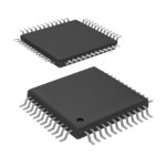 ADC10D020CIVSX/NOPB

ADC10D020CIVSX/NOPB is listed in the Analog To Digital Converters (ADC) range at ChipApex. The manufacturer field lists Texas Instruments. Its product description is IC…
Read More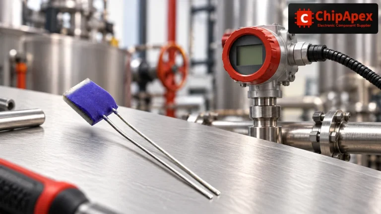
Compare Pt100 and Pt1000 RTDs, two-, three- and four-wire connections, excitation and self-heating. Build an error budget from element to reported temperature.
Read More
ADC10D020CIVSX/NOPB is listed in the Analog To Digital Converters (ADC) range at ChipApex. The manufacturer field lists Texas Instruments. Its product description is IC…
Read More
ADC10D020CIVSX/NOPB is listed in the Analog To Digital Converters (ADC) range at ChipApex. The manufacturer field lists Texas Instruments. Its product description is IC…
Read More
ADC10D020CIVSX/NOPB is listed in the Analog To Digital Converters (ADC) range at ChipApex. The manufacturer field lists Texas Instruments. Its product description is IC…
Read More
See how a MEMS gyroscope measures angular rate, why its angle estimate drifts, and which range, noise, interface and temperature specs to compare.
Read More
Learn why PTC resistance rises with temperature, how it differs from NTC, and which ratings matter for sensing and protection.
Read More
ADC10D020CIVSX/NOPB is listed in the Analog To Digital Converters (ADC) range at ChipApex. The manufacturer field lists Texas Instruments. Its product description is IC…
Read More
ADC10D020CIVSX/NOPB is listed in the Analog To Digital Converters (ADC) range at ChipApex. The manufacturer field lists Texas Instruments. Its product description is IC…
Read MoreADC10D020CIVSX/NOPB is listed in the Analog To Digital Converters (ADC) range at ChipApex. The manufacturer field lists Texas Instruments. Its product description is IC…
Read More
ADC10D020CIVSX/NOPB is listed in the Analog To Digital Converters (ADC) range at ChipApex. The manufacturer field lists Texas Instruments. Its product description is IC…
Read More
ADC10D020CIVSX/NOPB is listed in the Analog To Digital Converters (ADC) range at ChipApex. The manufacturer field lists Texas Instruments. Its product description is IC…
Read More
The activity of extra discounts on wholesale prices is in full swing…
Please fill in your contact information and we will send you the latest wholesale price list.




