 ChipApex | Global Electronic Components Supplier

SEARCH
Search Product
Search Post
— IC芯片 | 连接器 | 传感器 | 被动器件 —
Search productSearch post
— IC芯片 | 连接器 | 传感器 | 被动器件 —
Consult the customer manager about the wholesale price.
consultation hotline:86-132-6715-2157
email:[email protected]
Contact the product manager for consultation. One-stop consultation is available.
Do you want a lower wholesale price? Please send us your inquiry and we will reply immediately.
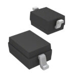
BAR6403WE6327HTSA1 is listed in the RF Diode range at ChipApex. The manufacturer field lists Infineon Technologies. Its product description is RF DIODE PIN 150V 250MW SOD323. Review the specifications below when checking this part for your BOM.
The BAR6403WE6327HTSA1 is a silicon PIN diode designed for low signal distortion in RF applications up to 3 GHz. It features a nominal 50 μm I-region width and a typical carrier lifetime of 1550 ns, resulting in low forward resistance and minimal distortion. The device operates with a maximum reverse voltage of 150 V and a forward current of 100 mA. Key electrical parameters include a typical capacitance of 0.61 pF at 0 V reverse bias (1 MHz) and a forward resistance of 2.7 Ω at 10 mA forward current (100 MHz). Packaged in the industry-standard SOD323 surface-mount format, it is qualified for industrial environments.
Verify component authenticity through official Infineon channels or authorized distributors. Confirm that the ordering suffix matches the required package and tape/reel specifications. Ensure handling procedures account for ESD sensitivity during storage and assembly. Cross-reference datasheet revision history to ensure compatibility with current design requirements.
Select this component when low distortion and high isolation are critical for frequencies up to 3 GHz. Evaluate thermal constraints based on the specified junction-to-soldering point thermal resistance. Consider the SOD323 footprint dimensions for PCB layout optimization. Verify that the operating temperature range meets the specific environmental conditions of the target application.
This part belongs to the BAR64 series of cost-optimized RF PIN diodes manufactured by Infineon Technologies. It is specifically engineered for surface mount applications requiring robust performance in switch and attenuator circuits. The product is designated as an individual datasheet item rather than part of a broader family document.
Publicly confirmed substitute part numbers are not available in the provided documentation. Designers should consult Infineon technical support for validated alternatives if this component becomes unavailable.
The typical capacitance is 0.2 pF at 0 V reverse bias for frequencies greater than or equal to 1 GHz.
The maximum junction temperature (TJ) is 150 °C.
The typical charge carrier lifetime (τrr) is 1550 ns, measured under specific test conditions including IF = 10 mA and IR = 6 mA.
Explore related parts through Diodes, Discrete Semiconductor Products, all product categories, ChipApex homepage.
 BAR6403WE6327HTSA1

Choose an AC to DC converter by input range, output demand, isolation, efficiency and thermal derating. Compare architectures and check installation needs.
Read More
BAR6403WE6327HTSA1 is listed in the RF Diode range at ChipApex. The manufacturer field lists Infineon Technologies. Its product description is RF DIODE PIN 150V…
Read More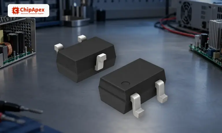
Learn how a diode conducts, how to identify anode and cathode, and when to choose rectifier, TVS, Zener or photodiode types for a circuit.
Read More
BAR6403WE6327HTSA1 is listed in the RF Diode range at ChipApex. The manufacturer field lists Infineon Technologies. Its product description is RF DIODE PIN 150V…
Read More
BAR6403WE6327HTSA1 is listed in the RF Diode range at ChipApex. The manufacturer field lists Infineon Technologies. Its product description is RF DIODE PIN 150V…
Read More
BAR6403WE6327HTSA1 is listed in the RF Diode range at ChipApex. The manufacturer field lists Infineon Technologies. Its product description is RF DIODE PIN 150V…
Read More
Find out when a bare shock switch needs a pull resistor, when an MCU internal pull-up is enough, and why sensor modules and piezo…
Read More
BAR6403WE6327HTSA1 is listed in the RF Diode range at ChipApex. The manufacturer field lists Infineon Technologies. Its product description is RF DIODE PIN 150V…
Read More
BAR6403WE6327HTSA1 is listed in the RF Diode range at ChipApex. The manufacturer field lists Infineon Technologies. Its product description is RF DIODE PIN 150V…
Read More
BAR6403WE6327HTSA1 is listed in the RF Diode range at ChipApex. The manufacturer field lists Infineon Technologies. Its product description is RF DIODE PIN 150V…
Read More
BAR6403WE6327HTSA1 is listed in the RF Diode range at ChipApex. The manufacturer field lists Infineon Technologies. Its product description is RF DIODE PIN 150V…
Read More
BAR6403WE6327HTSA1 is listed in the RF Diode range at ChipApex. The manufacturer field lists Infineon Technologies. Its product description is RF DIODE PIN 150V…
Read More
The activity of extra discounts on wholesale prices is in full swing…
Please fill in your contact information and we will send you the latest wholesale price list.




