ChipApex | Global Electronic Components Supplier

SEARCH
Search Product
Search Post
— IC芯片 | 连接器 | 传感器 | 被动器件 —
Search productSearch post
— IC芯片 | 连接器 | 传感器 | 被动器件 —
Consult the customer manager about the wholesale price.
consultation hotline:86-132-6715-2157
email:[email protected]
Contact the product manager for consultation. One-stop consultation is available.
Do you want a lower wholesale price? Please send us your inquiry and we will reply immediately.
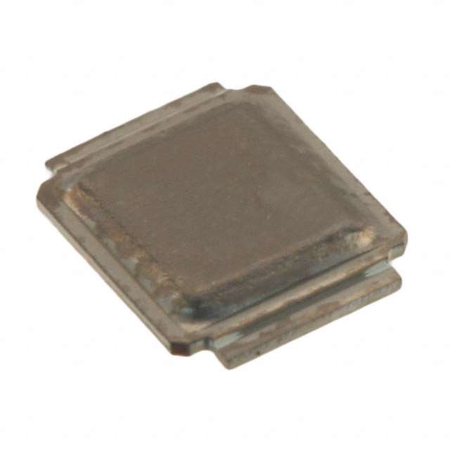
BSB012NE2LX is listed in the Single FETs, MOSFETs range at ChipApex. The manufacturer field lists Infineon Technologies. Its product description is MOSFET N-CH 25V 37A/170A 2WDSON. Review the specifications below when checking this part for your BOM.
The BSB012NE2LX is an n-Channel Power MOSFET from Infineon's OptiMOS™ family, designed for high power density and energy efficiency. It features a maximum drain-source voltage (VDS) of 25 V and a continuous drain current (ID) of 170 A at 25 °C case temperature. The device exhibits a maximum on-state resistance (RDS(on)) of 1.6 mΩ at VGS=4.5 V and 1.2 mΩ at VGS=10 V. Key dynamic parameters include a total gate charge (Qg) of 32 nC at VGS=10 V and an output charge (Qoss) of 35 nC. It operates within a junction temperature range of -40 °C to +150 °C.
Verify the specific ordering suffix and packaging configuration directly with the manufacturer or authorized distributors before procurement. Confirm that the component meets all required environmental standards, including RoHS compliance and halogen-free specifications, as these attributes are critical for final assembly processes. Ensure thermal management solutions align with the specified thermal resistance values provided in the datasheet.
Select this component when designing voltage regulator solutions for servers, datacom, and telecom applications requiring high efficiency and compact form factors. The low RDS(on) and fast switching characteristics make it suitable for synchronous control and sync FETs where EMI reduction is necessary. Evaluate the thermal performance against the application's heat dissipation requirements using the provided thermal resistance data.
This part belongs to the OptiMOS™ 25V series, which targets demanding voltage regulation standards in computing applications. It utilizes the MG-WDSON-2 package to provide flexibility in optimizing space and cost. The technology focuses on achieving class-leading power density through superior thermal resistance and optimized electrical characteristics compared to standard MOSFETs.
Consult official cross-reference tools or contact Infineon Technologies for verified substitute part numbers. Do not assume compatibility based solely on similar voltage or current ratings; verify pinout, package dimensions, and electrical parameters against the original specification.
The datasheet states the device is qualified according to JEDEC standards for target applications such as servers and datacom. Use in automotive, aviation, or aerospace systems requires express written approval from Infineon Technologies.
The maximum pulsed drain current (ID,pulse) is rated at 400 A at a case temperature of 25 °C.
Explore related parts through FETs, MOSFETs, Transistors, Discrete Semiconductor Products, all product categories.
 BSB012NE2LX
BSB012NE2LX is listed in the Single FETs, MOSFETs range at ChipApex. The manufacturer field lists Infineon Technologies. Its product description is MOSFET N-CH 25V…
Read More
BSB012NE2LX is listed in the Single FETs, MOSFETs range at ChipApex. The manufacturer field lists Infineon Technologies. Its product description is MOSFET N-CH 25V…
Read More
BSB012NE2LX is listed in the Single FETs, MOSFETs range at ChipApex. The manufacturer field lists Infineon Technologies. Its product description is MOSFET N-CH 25V…
Read More
BSB012NE2LX is listed in the Single FETs, MOSFETs range at ChipApex. The manufacturer field lists Infineon Technologies. Its product description is MOSFET N-CH 25V…
Read MoreBSB012NE2LX is listed in the Single FETs, MOSFETs range at ChipApex. The manufacturer field lists Infineon Technologies. Its product description is MOSFET N-CH 25V…
Read More
BSB012NE2LX is listed in the Single FETs, MOSFETs range at ChipApex. The manufacturer field lists Infineon Technologies. Its product description is MOSFET N-CH 25V…
Read More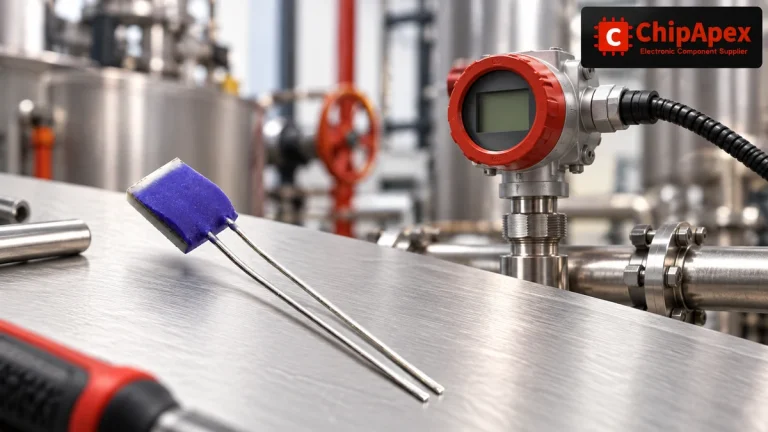
Compare Pt100 and Pt1000 RTDs, two-, three- and four-wire connections, excitation and self-heating. Build an error budget from element to reported temperature.
Read More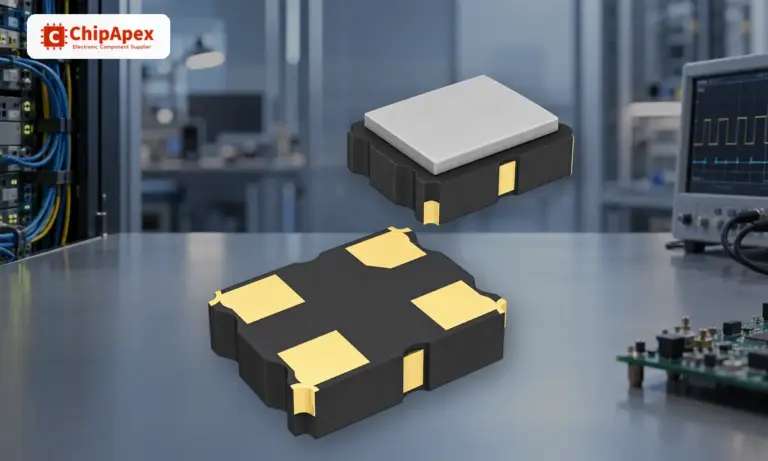
Understand how oscillators generate timing signals, how they differ from crystals, and which frequency, output and stability specs matter when choosing one.
Read More
BSB012NE2LX is listed in the Single FETs, MOSFETs range at ChipApex. The manufacturer field lists Infineon Technologies. Its product description is MOSFET N-CH 25V…
Read More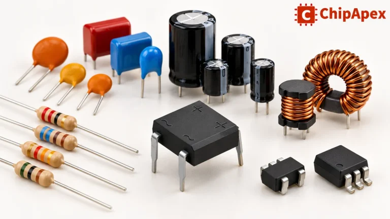
Explore electronic component types, functions, packages and datasheets. Learn selection, replacement and BOM checks before ordering parts for your PCB.
Read More
BSB012NE2LX is listed in the Single FETs, MOSFETs range at ChipApex. The manufacturer field lists Infineon Technologies. Its product description is MOSFET N-CH 25V…
Read More
BSB012NE2LX is listed in the Single FETs, MOSFETs range at ChipApex. The manufacturer field lists Infineon Technologies. Its product description is MOSFET N-CH 25V…
Read More
The activity of extra discounts on wholesale prices is in full swing…
Please fill in your contact information and we will send you the latest wholesale price list.