 ChipApex | Global Electronic Components Supplier

SEARCH
Search Product
Search Post
— IC芯片 | 连接器 | 传感器 | 被动器件 —
Search productSearch post
— IC芯片 | 连接器 | 传感器 | 被动器件 —
Consult the customer manager about the wholesale price.
consultation hotline:86-132-6715-2157
email:chipapex@foxmail.com
Contact the product manager for consultation. One-stop consultation is available.
Do you want a lower wholesale price? Please send us your inquiry and we will reply immediately.
CDCF2510PWG4 is listed in the Application Specific Clock/Timing range at ChipApex. The manufacturer field lists Texas Instruments. Its product description is IC 3.3V PLL CLK-DRVR 24-TSSOP. Review the specifications below when checking this part for your BOM.
The CDCF2510PWG4 is a 3.3-V phase-lock loop (PLL) clock driver manufactured by Texas Instruments, housed in a 24-pin TSSOP package. It distributes one clock input to a bank of ten outputs with low skew and low jitter characteristics. The device operates at frequencies between 25 MHz and 140 MHz and includes integrated series-damping resistors for point-to-point loads. It requires no external RC network due to an on-chip loop filter. The G input enables or disables all outputs, while the FBIN terminal synchronizes outputs to the clock input.
Verify that the component matches the LIFEBUY status indicated in the packaging information addendum. Confirm the specific ordering suffix corresponds to the desired package type and environmental compliance before procurement. Ensure design compatibility with the specified operating temperature range of 0°C to 85°C.
Select this device when a 3.3-V PLL clock driver is required for synchronous DRAM buses. Ensure the application frequency falls within the 25 MHz to 140 MHz range. Verify that the PCB layout accommodates the 24-pin TSSOP package and allows for proper connection of the FBOUT to FBIN feedback loop.
The CDCF2510PWG4 belongs to the CDCF2510 family of high-performance, low-skew, low-jitter PLL clock drivers. It is specifically engineered for synchronous DRAM applications where precise phase alignment and minimal jitter are critical. The 'G4' suffix indicates RoHS-compliant manufacturing.
The datasheet explicitly recommends using the CDCVF2510A as a replacement for this device.
Explore related parts through Clock/Timing, Integrated Circuits (ICs), all product categories, ChipApex homepage.
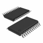 CDCF2510PWG4

CDCF2510PWG4 is listed in the Application Specific Clock/Timing range at ChipApex. The manufacturer field lists Texas Instruments. Its product description is IC 3.3V PLL…
Read More
CDCF2510PWG4 is listed in the Application Specific Clock/Timing range at ChipApex. The manufacturer field lists Texas Instruments. Its product description is IC 3.3V PLL…
Read More
Select power transformers by input frequency, secondary VA, rectifier load, isolation, regulation and inrush. Build a clearer specification for your next RFQ.
Read More
CDCF2510PWG4 is listed in the Application Specific Clock/Timing range at ChipApex. The manufacturer field lists Texas Instruments. Its product description is IC 3.3V PLL…
Read More
CDCF2510PWG4 is listed in the Application Specific Clock/Timing range at ChipApex. The manufacturer field lists Texas Instruments. Its product description is IC 3.3V PLL…
Read More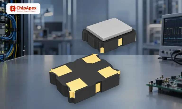
Understand how oscillators generate timing signals, how they differ from crystals, and which frequency, output and stability specs matter when choosing one.
Read More
Compare RC, crystal and MEMS oscillator circuits. Check ppm, jitter, load capacitance, startup margin and output compatibility before choosing a clock source.
Read More
CDCF2510PWG4 is listed in the Application Specific Clock/Timing range at ChipApex. The manufacturer field lists Texas Instruments. Its product description is IC 3.3V PLL…
Read More
CDCF2510PWG4 is listed in the Application Specific Clock/Timing range at ChipApex. The manufacturer field lists Texas Instruments. Its product description is IC 3.3V PLL…
Read More
CDCF2510PWG4 is listed in the Application Specific Clock/Timing range at ChipApex. The manufacturer field lists Texas Instruments. Its product description is IC 3.3V PLL…
Read More
CDCF2510PWG4 is listed in the Application Specific Clock/Timing range at ChipApex. The manufacturer field lists Texas Instruments. Its product description is IC 3.3V PLL…
Read More
CDCF2510PWG4 is listed in the Application Specific Clock/Timing range at ChipApex. The manufacturer field lists Texas Instruments. Its product description is IC 3.3V PLL…
Read More
The activity of extra discounts on wholesale prices is in full swing…
Please fill in your contact information and we will send you the latest wholesale price list.





