ChipApex | Global Electronic Components Supplier

SEARCH
Search Product
Search Post
— IC芯片 | 连接器 | 传感器 | 被动器件 —
Search productSearch post
— IC芯片 | 连接器 | 传感器 | 被动器件 —
Consult the customer manager about the wholesale price.
consultation hotline:86-132-6715-2157
email:[email protected]
Contact the product manager for consultation. One-stop consultation is available.
Do you want a lower wholesale price? Please send us your inquiry and we will reply immediately.
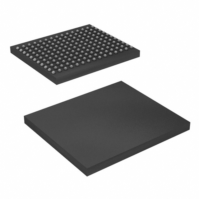
CY7C1268KV18-400BZXC is listed in the Memory IC range at ChipApex. The manufacturer field lists Cypress Semiconductor Corp. Its product description is IC SRAM 36MBIT PARALLEL 165FBGA. Review the specifications below when checking this part for your BOM.
The CY7C1268KV18-400BZXC is a 36-Mbit synchronous pipelined SRAM featuring DDR II+ architecture. It offers a density of 2 M × 18 and supports maximum operating frequencies up to 400 MHz, with data transfer rates reaching 800 MHz via double data rate interfaces. The device operates within a core voltage range of 1.7 V to 1.9 V and an I/O voltage range of 1.4 V to VDD. It utilizes a 165-ball FBGA package (13 × 15 × 1.4 mm) and provides a read latency of 2.5 cycles when the DOFF pin is asserted HIGH.
Verify component authenticity through authorized Infineon or Cypress distributors. Confirm package marking matches the specified 165-ball FBGA configuration. Ensure supply chain documentation aligns with current product lifecycle status. Request relevant quality certificates such as RoHS compliance and material declarations prior to finalizing acquisition orders.
Select this component for designs requiring 36-Mbit capacity with specific 2 M × 18 organization. Evaluate system timing constraints against the 2.5-cycle read latency specification. Consider power supply requirements for both core and I/O domains. Assess PCB layout needs for the 165-ball FBGA footprint and impedance matching resistor placement on the ZQ pin.
This part belongs to the CY7C1268KV18 family of DDR II+ SRAMs manufactured by Infineon Technologies. It shares architectural similarities with other members like the CY7C1270KV18 but differs in memory organization. The series targets high-performance embedded systems where low latency and high throughput are critical design parameters.
Public confirmed substitute part numbers: None identified.
Explore related parts through Memory, Integrated Circuits (ICs), all product categories, ChipApex homepage.
 CY7C1268KV18-400BZXC
Choose a rocker switch by AC/DC ratings, contact arrangement, illumination, panel fit and sealing. Get practical checks for engineering and component sourcing.
Read More
Choose logic inverter ICs by thresholds, supply, output drive and delay. Compare standard and Schmitt-trigger inputs, power sequencing and replacement checks.
Read More
CY7C1268KV18-400BZXC is listed in the Memory IC range at ChipApex. The manufacturer field lists Cypress Semiconductor Corp. Its product description is IC SRAM 36MBIT…
Read More
CY7C1268KV18-400BZXC is listed in the Memory IC range at ChipApex. The manufacturer field lists Cypress Semiconductor Corp. Its product description is IC SRAM 36MBIT…
Read More
CY7C1268KV18-400BZXC is listed in the Memory IC range at ChipApex. The manufacturer field lists Cypress Semiconductor Corp. Its product description is IC SRAM 36MBIT…
Read More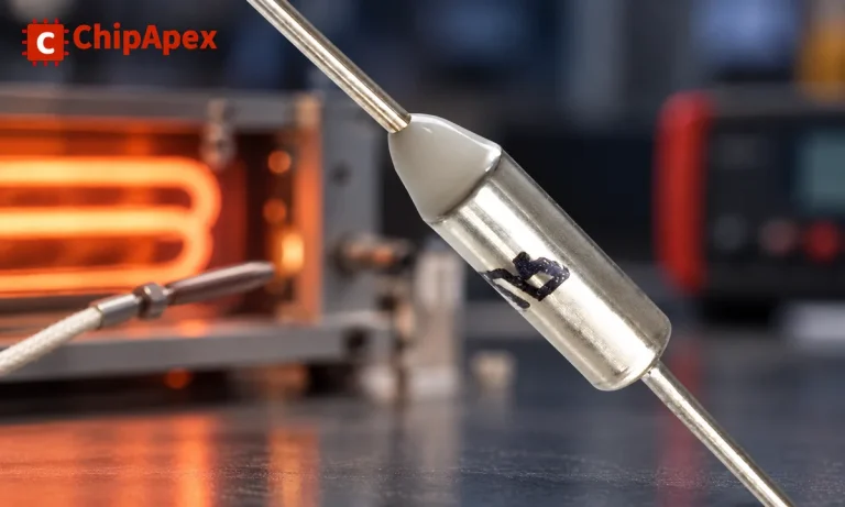
Understand thermal fuse operation, Tf, Th and Tm, electrical ratings and mounting. Check temperature limits and replacement requirements for your design.
Read More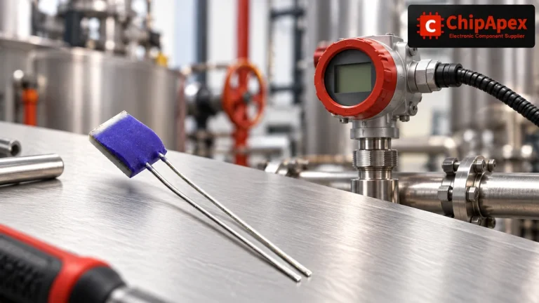
Compare Pt100 and Pt1000 RTDs, two-, three- and four-wire connections, excitation and self-heating. Build an error budget from element to reported temperature.
Read More
CY7C1268KV18-400BZXC is listed in the Memory IC range at ChipApex. The manufacturer field lists Cypress Semiconductor Corp. Its product description is IC SRAM 36MBIT…
Read More
CY7C1268KV18-400BZXC is listed in the Memory IC range at ChipApex. The manufacturer field lists Cypress Semiconductor Corp. Its product description is IC SRAM 36MBIT…
Read More
CY7C1268KV18-400BZXC is listed in the Memory IC range at ChipApex. The manufacturer field lists Cypress Semiconductor Corp. Its product description is IC SRAM 36MBIT…
Read More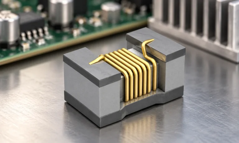
See when an inductor behaves linearly, how DC bias and saturation reduce inductance, and which current and temperature curves to check.
Read More
CY7C1268KV18-400BZXC is listed in the Memory IC range at ChipApex. The manufacturer field lists Cypress Semiconductor Corp. Its product description is IC SRAM 36MBIT…
Read More
The activity of extra discounts on wholesale prices is in full swing…
Please fill in your contact information and we will send you the latest wholesale price list.