ChipApex | Global Electronic Components Supplier

SEARCH
Search Product
Search Post
— IC芯片 | 连接器 | 传感器 | 被动器件 —
Search productSearch post
— IC芯片 | 连接器 | 传感器 | 被动器件 —
Consult the customer manager about the wholesale price.
consultation hotline:86-132-6715-2157
email:[email protected]
Contact the product manager for consultation. One-stop consultation is available.
Do you want a lower wholesale price? Please send us your inquiry and we will reply immediately.
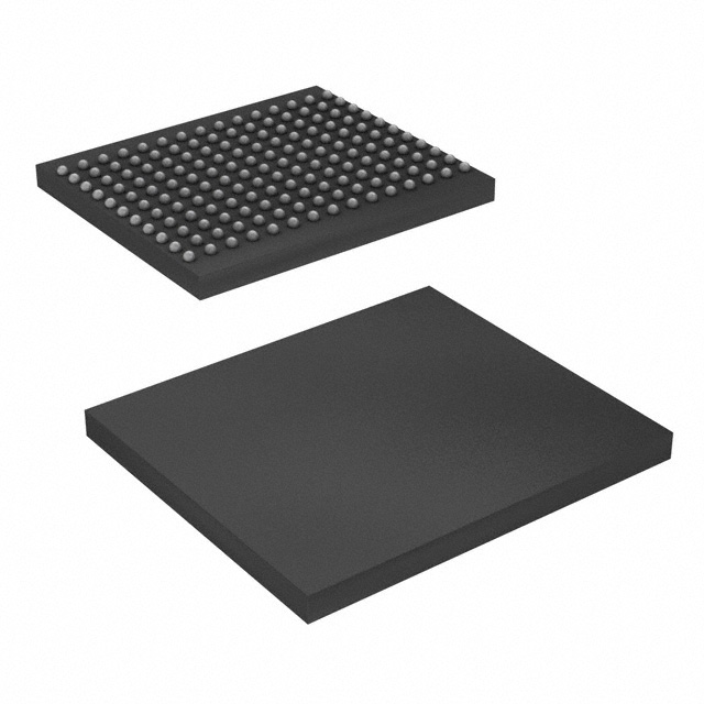
CY7C14251KV18-250BZI is listed in the Memory IC range at ChipApex. The manufacturer field lists Infineon Technologies. Its product description is IC SRAM 36MBIT PAR 165FBGA. Review the specifications below when checking this part for your BOM.
The CY7C14251KV18-250BZI is a 36-Mbit QDR II SRAM with a 4M x 9 organization. It supports a maximum clock frequency of 250 MHz and operates within a voltage range of 1.7 V to 1.9 V for the core supply. The device features separate independent read and write data ports, enabling concurrent transactions without bus turnaround delays. It utilizes double data rate interfaces on both ports, transferring data at 666 MHz relative to the 333 MHz internal clock. The component is housed in a 165-ball FBGA package.
Verify the specific suffix BZI against official Infineon documentation to confirm lead-free status and industrial temperature rating. Confirm that the 250 MHz speed grade matches system timing requirements. Ensure compatibility with the 165-ball FBGA footprint and verify power supply constraints for both core and I/O voltages prior to integration.
Select this component when a 4M x 9 organization is required alongside QDR II architecture benefits. Consider the 250 MHz speed grade if system latency targets are met by the specified access times. Evaluate the need for separate port selects if depth expansion beyond single-device capacity is planned for the design.
This part belongs to the Cypress/Infineon QDR II SRAM family, which includes variants such as the CY7C14101KV18, CY7C14121KV18, and CY7C14141KV18. These devices share common architectural features like dual-port independence and echo clock generation but differ in bit-width configurations ranging from x8 to x36. The CY7C14251KV18 specifically addresses applications needing 9-bit word widths.
When DOFF is asserted HIGH, the device operates with a 1.5-cycle read latency using the PLL. When DOFF is LOW, the PLL is disabled, and the device behaves in QDR I mode with a 1-cycle read latency.
The ZQ pin is used for output impedance matching. An external resistor connects ZQ to ground to tune the output drivers to the system data bus impedance, typically set to 0.2 times the line impedance.
Explore related parts through Memory, Integrated Circuits (ICs), all product categories, ChipApex homepage.
 CY7C14251KV18-250BZI
CY7C14251KV18-250BZI is listed in the Memory IC range at ChipApex. The manufacturer field lists Infineon Technologies. Its product description is IC SRAM 36MBIT PAR…
Read More
CY7C14251KV18-250BZI is listed in the Memory IC range at ChipApex. The manufacturer field lists Infineon Technologies. Its product description is IC SRAM 36MBIT PAR…
Read More
Understand RF attenuator dB values, fixed and programmable types, impedance, power limits and noise tradeoffs before choosing parts for an RF signal path.
Read More
CY7C14251KV18-250BZI is listed in the Memory IC range at ChipApex. The manufacturer field lists Infineon Technologies. Its product description is IC SRAM 36MBIT PAR…
Read More
Understand UART protocol framing, baud rate and electrical interfaces. Learn 8N1 timing, TX/RX wiring, buffering and practical troubleshooting steps.
Read More
CY7C14251KV18-250BZI is listed in the Memory IC range at ChipApex. The manufacturer field lists Infineon Technologies. Its product description is IC SRAM 36MBIT PAR…
Read More
CY7C14251KV18-250BZI is listed in the Memory IC range at ChipApex. The manufacturer field lists Infineon Technologies. Its product description is IC SRAM 36MBIT PAR…
Read More
CY7C14251KV18-250BZI is listed in the Memory IC range at ChipApex. The manufacturer field lists Infineon Technologies. Its product description is IC SRAM 36MBIT PAR…
Read More
CY7C14251KV18-250BZI is listed in the Memory IC range at ChipApex. The manufacturer field lists Infineon Technologies. Its product description is IC SRAM 36MBIT PAR…
Read More
Choose a rocker switch by AC/DC ratings, contact arrangement, illumination, panel fit and sealing. Get practical checks for engineering and component sourcing.
Read More
Choose LED drivers by current, string voltage, dimming and thermal limits. Understand constant-current operation and the checks needed for your load.
Read More
Choose an ADC converter by resolution, sample rate, noise and input design. Review practical tradeoffs and prepare component requirements for ChipApex.
Read More
The activity of extra discounts on wholesale prices is in full swing…
Please fill in your contact information and we will send you the latest wholesale price list.